Solid-state relay

A relay and collector technology, applied in the design field of solid state relays, can solve the problems of insufficient control, poor anti-interference ability, increased chip area and wiring difficulty, etc., to avoid misdirection, strong anti-interference ability, and increased area.

Inactive Publication Date: 2012-03-28
UNIV OF ELECTRONICS SCI & TECH OF CHINA
View PDF7 Cites 13 Cited by
  • Summary
  • Abstract
  • Description
  • Claims
  • Application Information

AI Technical Summary

Problems solved by technology

This solution effectively reduces the turn-on time, but due to the introduction of capacitors and the need for output power, the chip area and the difficulty of wiring are inevitably increased. In addition, the control of the slope of the falling edge is also slightly insufficient, and the anti-interference ability is poor.

Method used


Image

  • Solid-state relay
  • Solid-state relay
  • Solid-state relay

Examples


Embodiment 1

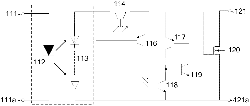
[0030] An embodiment of the solid state relay according to the present invention is as follows: figure 1 shown in Example 1. Specifically, it includes a light-emitting element 112 connected between the relay input terminals 111 and 111a;

[0031] A photovoltaic diode array 113 that generates photovoltaic output when coupled with the light signal of the light-emitting element;

[0032] A normally-on metal oxide field effect transistor 120 connected between the output terminals of the relay;

[0033] Also includes,

[0034] An accelerated charging circuit composed of phototransistors 114, wherein the emitter of the phototransistor 114 is connected to the gate of the output normally-on metal oxide field effect transistor 120, and the collector is connected to the first end of the photovoltaic diode array 113;

[0035] An acceleration discharge circuit composed of two PNP triodes, an NPN triode 119 and a phototransistor 118, wherein the two PNP triodes are specifically the firs...

Embodiment 2

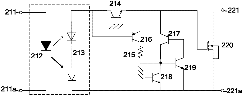
[0040] like figure 2 As shown, as a preferred mode of the first embodiment, the relay further includes a resistor 215, wherein the resistor 215 is connected between the collector of the first PNP transistor 216 and the collector of the second PNP transistor 217. Here, the introduction of the resistor 215 can reduce the probability of mis-conduction of the trigger current caused by the voltage fluctuation of the output terminal, and the size of the resistor 215 determines the size of the current triggered by the first PNP transistor 216 . For the specific working process, refer to Embodiment 1.

Embodiment 3

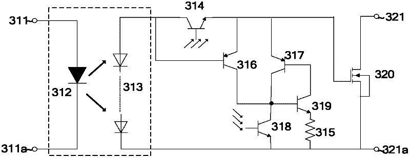
[0042] like image 3 As shown, as another preferred mode of the first embodiment, here, the relay further includes a resistor 315 , and the resistor 315 is connected between the emitter of the NPN transistor 319 and the emitter of the phototransistor 318 . This change can reduce the false turn-on, and at the same time, the impedance of the channel becomes larger during the discharge, so that the slope of the falling edge becomes slower, which improves the anti-noise capability. The specific working process can also refer to Embodiment 1.


PUM


Abstract

The invention discloses a solid-state relay which comprises a light-emitting element, a photovoltaic diode array, one or two normally open metallic oxide field effect transistors which are arranged between output terminals of the relay, an accelerated charging circuit formed by photoelectric triodes, and an accelerated leakage circuit formed by two PNP triodes, an NPN triode and a photoelectric triode. The solid-state relay can be realized in a way that the output metallic oxide field effect transistor gate capacitance is charged and discharged, the purpose of fast connection and disconnection on the relay can be achieved by using the circuit structure, the photoelectric triodes are led, the circuit is at a state of illumination when the output metallic oxide field effect transistor gate capacitance is charged, and the photoelectric triodes of the accelerated charging circuit are at a state of low resistivity. The relay is simple in structure, and improves the anti-interference capability when the connection time is not added.

Description

technical field [0001] The invention belongs to the technical field of electrical appliances and in particular relates to the design of a solid state relay. Background technique [0002] Solid State Relays (SSR) is a non-contact electronic switch, which uses the switching characteristics of electronic components (such as switching transistors, triacs and other semiconductor devices) to achieve non-contact and non-sparking connection and switching. The purpose of disconnecting the circuit is to add a DC or pulse signal to its input terminal, and the output terminal can change from the off state to the on state (blocking state when there is no signal), that is, when a voltage is applied between the control pins, The solid state relay is turned on, and when the applied voltage between the control pins is removed, the solid state relay is disconnected, thereby controlling a larger load. [0003] The turn-off control circuit of the solid state relay introduced in US Patent No. 4...

Claims


Application Information

Patent Timeline
Patent Type & Authority Applications(China)
IPC IPC(8): H03K17/56
Inventor 张有润吴浩然张波
Owner UNIV OF ELECTRONICS SCI & TECH OF CHINA
Why Eureka
Try Eureka