Dye-sensitized solar cell and dye-sensitized solar cell module
A solar cell and dye-sensitized technology, which is applied in the field of dye-sensitized solar cells and dye-sensitized solar cell modules, can solve problems such as increased internal resistance, reduced short-circuit current, and reduced photoelectric conversion efficiency, and achieves high conversion efficiency.
- Summary
- Abstract
- Description
- Claims
- Application Information
AI Technical Summary
Problems solved by technology
Method used
Image

Examples
Embodiment approach 1-1
[0039] By laminating at least a catalyst layer, a porous insulating layer containing an electrolyte therein, and a porous semiconductor layer having adsorbed a sensitizing dye and containing an electrolyte therein on the first conductive layer in this order, and laminating the second conductive layer on the a structure formed between the porous insulating layer and the porous semiconductor layer (Embodiment 1-1 to be described below); and
[0040]By laminating at least a catalyst layer, a porous insulating layer containing an electrolyte therein, and a porous semiconductor layer adsorbed with a sensitizing dye and containing an electrolyte therein on the first conductive layer in this order, and further laminating the second conductive layer on the The structure formed on the above-mentioned porous semiconductor layer (Embodiment 2-1 to be described below).
[0041] In addition, the solar cell of the present invention is characterized in that at least a porous semiconductor la...
Embodiment approach 3-1
[0043] By laminating a porous semiconductor layer having adsorbed at least a sensitizing dye and containing an electrolyte therein, a porous insulating layer containing an electrolyte therein, a second conductive layer, and a catalyst layer on a first conductive layer, and forming the porous insulating layer, a structure in which the second conductive layer and the catalyst layer are laminated in this order (Embodiment 3-1 to be described below); and
[0044] By laminating a porous semiconductor layer having adsorbed at least a sensitizing dye and containing an electrolyte therein, a porous insulating layer containing an electrolyte therein, a second conductive layer, and a catalyst layer on a first conductive layer, and forming the porous insulating layer, A structure in which the catalyst layer and the second conductive layer are stacked in this order (Embodiment 4-1 to be described below).
[0045] In the following, refer to Figure 1-4 and 6-9, embodiment 1-2 obtained by ...
Embodiment approach 1-2
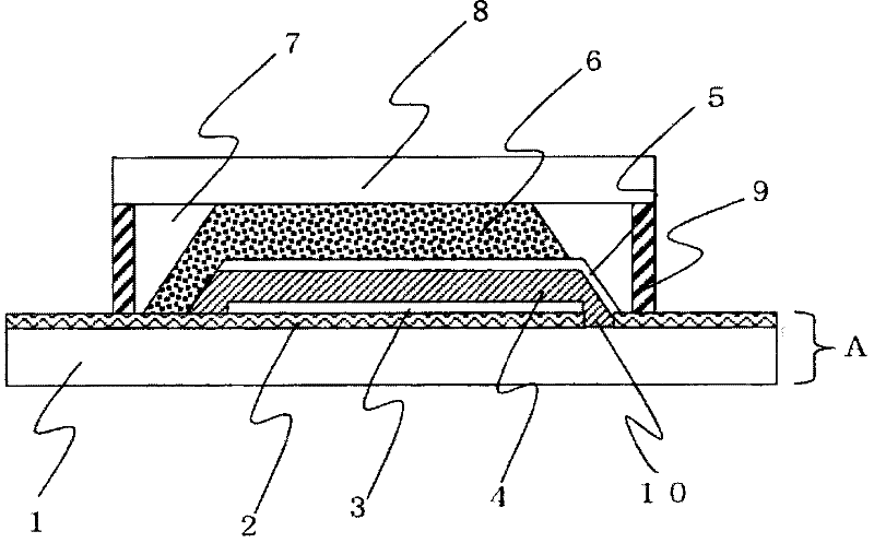
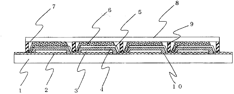
[0152] figure 2 is a schematic cross-sectional view showing the layer structure of main components of a solar cell module (Embodiment 1-2) obtained by electrically connecting a plurality of solar cells of the present invention (Embodiment 1-1) in series.
[0153] This solar cell module can be manufactured as follows.
[0154] First, the first conductive layer formed on the substrate 1 is patterned at prescribed intervals by a laser scribing method to form a plurality of scribe lines in which the conductive layer is removed. Accordingly, a plurality of first conductive layers 2 electrically isolated from each other are formed, and a solar cell formation region is provided on each first conductive layer 2 .
[0155] Among the plurality of first conductive layers 2, the first conductive layer 2 at one end in the direction perpendicular to the scribe line 10 is formed to have a smaller width, and no solar cell is formed on the first conductive layer 2 with the smaller width. on...
PUM
| Property | Measurement | Unit |
|---|---|---|
| thickness | aaaaa | aaaaa |
| thickness | aaaaa | aaaaa |
| thickness | aaaaa | aaaaa |
Abstract
Description
Claims
Application Information