
Method for growing large area of layer-number-controllable graphene at low temperature through chemical vapor deposition (CVD) method by using polystyrene solid state carbon source

A solid carbon source, polystyrene technology, applied in gaseous chemical plating, coating, metal material coating process, etc., can solve the problems of small graphene area, many defects, poor crystal quality, etc., and achieve cost reduction. Effect

Inactive Publication Date: 2012-04-04
NANJING UNIV OF AERONAUTICS & ASTRONAUTICS
View PDF1 Cites 35 Cited by
  • Summary
  • Abstract
  • Description
  • Claims
  • Application Information

AI Technical Summary

Problems solved by technology

However, the graphene directly deposited by these methods has a small area, poor crystal quality, and many defects.

Method used

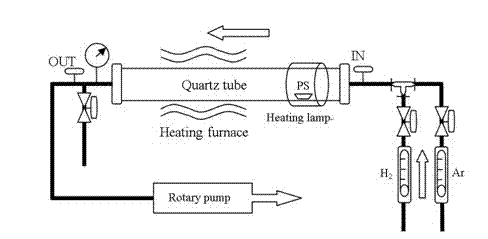

Image

  • Method for growing large area of layer-number-controllable graphene at low temperature through chemical vapor deposition (CVD) method by using polystyrene solid state carbon source
  • Method for growing large area of layer-number-controllable graphene at low temperature through chemical vapor deposition (CVD) method by using polystyrene solid state carbon source
  • Method for growing large area of layer-number-controllable graphene at low temperature through chemical vapor deposition (CVD) method by using polystyrene solid state carbon source

Examples


Embodiment 1

[0036] Example 1: Large-area single-layer graphene was grown at low temperature using a polystyrene solid carbon source.

[0037] (1) Cu is used as the substrate, and the surface of the copper substrate is treated by mechanical polishing and electrochemical polishing successively to make the surface roughness below 5nm; the mechanical polishing speed is 800 rpm. The electrochemical workstation was used as the polishing power supply, and the Ag / AgCl electrode was selected as the reference electrode; the electrochemical polishing solution was a mixture of 85% phosphoric acid and polyethylene glycol with a volume ratio of 3:1. The copper sheet to be polished is placed on the positive electrode, and the copper sheet is used as the negative electrode; the electrochemical polishing voltage is 1~2V, and the polishing time is 1800s;

[0038] (2) After electrochemical polishing, ultrasonically clean the copper foil with acetone for 10 minutes, then ultrasonically clean it with 25% hydr...

Embodiment 2

[0045] Embodiment 2: Increase the weight of the polystyrene solid carbon source in Embodiment 1 to 30 mg; then repeat the process of Embodiment 1.

[0046] Example results: the transmittance test shows that the transmittance of the graphene thin layer prepared at 600° C. by 30 mg of the solid source reaches 93.5%. for bilayer graphene. Optical photographs show that the large-area graphene chemically transferred onto the glass substrate does not have any macroscopic damage. It is a complete double-layer graphene with an area of ​​1cm*2cm.

Embodiment 3

[0047] Embodiment 3: Increase the weight of the polystyrene solid carbon source in Embodiment 1 to 45 mg. Then repeat the process of embodiment one.

[0048] Example results: the transmittance test shows that the transmittance of the graphene thin layer prepared at 600° C. by 45 mg of the solid source reaches 90.3%. for three-layer graphene. Optical photographs show that the large-area graphene chemically transferred onto the glass substrate does not have any macroscopic damage. It is a complete three-layer graphene with an area of ​​1cm*2cm.

[0049] By the implementation result of embodiment 1, embodiment 2 and embodiment 3, illustrate by controlling polystyrene solid carbon source weight

[0050] The low-temperature preparation of graphene with different layers has high reliability, and can guarantee the preparation of graphene with stable quality and controllable layers.


PUM

PropertyMeasurementUnit
Surface roughnessaaaaaaaaaa

Abstract

The invention belongs to the field of new material preparation, resumptively relates to a method for growing a large area of graphene at a low temperature through a chemical vapor deposition (CVD) method by using a polystyrene solid state carbon source. The graphene grown by adopting the method has a smooth and level surface and the layer number of the graphene is controllable. The invention provides the method for preparing a layer-number-controllable graphene thin layer in a low temperature condition by adopting the low-cost solid state carbon source. Compared with a traditional method for preparing the graphene thin layer by adopting a high temperature CVD method, the manufacturing cost of the graphene thin layer is greatly reduced, and the method disclosed by the invention has enormous application potential in the aspects of high temperature, high frequency, large power, photoelectron, radiation-resistant electronic devices and the like.

Description

technical field [0001] The invention belongs to the field of new material preparation. It is summarized as a method for growing large-area graphene by chemical vapor deposition at low temperature using a polystyrene solid carbon source. Specifically, when using mechanically and electrochemically double-polished copper foil as a substrate, high-quality graphene can be prepared at low temperature; by controlling the weight of polystyrene solid carbon source, the graphene layer at low temperature can be realized Number controllable growth. [0002] Background technique [0003] Graphene is a single layer of atomically thick graphite with a two-dimensional honeycomb network structure. Due to the existence of π orbitals in the graphene sheet plane, electrons can move freely in the crystal, which makes graphene have very excellent electron transport properties. Due to its excellent mechanical, thermal, electrical and magnetic properties, graphene is expected to be widely used ...

Claims


Application Information

Patent Timeline
IPC IPC(8): C23C16/26C23C16/52
Inventor 沈鸿烈吴天如孙雷
Owner NANJING UNIV OF AERONAUTICS & ASTRONAUTICS
Learn More