Exposure method adopting lithography machine

An exposure method and a lithography machine technology, which are applied in the field of lithography machine exposure, can solve the problems of production capacity decline, equipment utilization rate reduction, increase, etc., achieve good process registration accuracy, prevent silicon wafer deformation, and increase equipment utilization rate Effect

Inactive Publication Date: 2012-04-11
SHANGHAI HUALI MICROELECTRONICS CORP
View PDF6 Cites 7 Cited by
  • Summary
  • Abstract
  • Description
  • Claims
  • Application Information

AI Technical Summary

Problems solved by technology

from figure 2 It can be seen from the figure that if the method of the prior art is used for photolithography, the continuously exposed silicon wafers will continuously increase the drift of the registration accuracy between the silicon wafers due to the heating of the silicon wafer stage.
[0006] A common solution is to control the registration accuracy by intermittently cooling the wafer stage during the wafer exposure process, but this leads to lower throughput and lower equipment utilization
In addition, since the temperature is continuously accumulated with exposure, batch-to-batch and wafer-to-wafer differences are unavoidable even with intermittent cooling

Method used


Image

  • Exposure method adopting lithography machine
  • Exposure method adopting lithography machine
  • Exposure method adopting lithography machine

Examples


Embodiment Construction

[0024] Embodiments of the present invention will be described in detail below. It should be noted that the embodiments described here are for illustration only, and are not intended to limit the present invention.

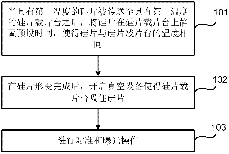
[0025] figure 1 An exemplary flow chart showing the exposure method of the lithography machine of the present invention includes the following steps 101-103 performed during the continuous operation of the lithography machine:

[0026] Step 101, after the silicon wafer with the first temperature is transferred to the silicon wafer loading table with the second temperature, the silicon wafer is placed on the silicon wafer loading table for a preset time, so that the silicon wafer and the silicon wafer loading table The temperature of the table is the same. The process of placing the silicon wafer on the silicon wafer stage for a preset time is equivalent to a process of temperature equilibrium, and the deformation of the silicon wafer is released during this proc...


PUM


Abstract

The invention discloses an exposure method adopting a lithography machine. The method comprises the following steps executed in the continuous working process of the lithography machine: 101. ensuring silicon wafers to stand for a preset time on a silicon wafer carrying stage to ensure the temperature of the silicon wafers to be the same as the temperature of the silicon wafer carrying stage after the silicon wafers with a first temperature are transferred to the silicon wafer carrying stage with a second temperature; 102. opening vacuum equipment to ensure the silicon wafer carrying stage to attract the silicon wafers after silicon wafer deformation is completed; and 103. carrying out alignment and exposure operations. The method provided by the invention has the following beneficial effects that: the process alignment precision can be improved; high homogeneity between silicon wafers and between batches is realized in the continuous working process of the lithography machine; and the equipment utilization rate can be improved.

Description

technical field [0001] The invention relates to semiconductor technology, in particular to an exposure method for a photolithography machine. Background technique [0002] At present, with the continuous improvement of integrated circuit manufacturing technology and the continuous shrinking of line width in lithography technology, the area of ​​semiconductor devices is becoming smaller and smaller. The layout of semiconductors has evolved from ordinary single-function separation devices to integrated high-density multi-functional Integrated circuits; from the initial integrated circuit (Integrated Circuit, referred to as IC) to large scale integrated circuit (Large Scale Integration, referred to as LSI), very large scale integrated circuit (Very Large Scale Integration, referred to as VLSI), until today's ultra-large scale Integrated circuit (Ultra Large Scale Integration, referred to as ULSI), the area of ​​the device is further reduced, and the function is more comprehensi...

Claims


Application Information

Patent Timeline
Patent Type & Authority Applications(China)
IPC IPC(8): G03F7/20
Inventor 朱骏陈力钧
Owner SHANGHAI HUALI MICROELECTRONICS CORP
Why Eureka
Try Eureka