
Method for manufacturing silicon nitride film with high tensile stress

A technology of silicon nitride film and tensile stress, which is applied in semiconductor/solid-state device manufacturing, electrical components, circuits, etc., can solve the problems of high cost, inability to meet high stress, complex manufacturing process, etc., and achieve the effect of increasing tensile stress

Active Publication Date: 2013-12-04
SHANGHAI HUALI MICROELECTRONICS CORP
View PDF3 Cites 0 Cited by
  • Summary
  • Abstract
  • Description
  • Claims
  • Application Information

AI Technical Summary

Problems solved by technology

The maximum stress of the silicon nitride film manufactured by this method does not exceed 1.8GPa, which cannot meet the requirements of high stress
[0005] In addition, the cost of making high-stress silicon nitride films is still relatively high, and the manufacturing process is relatively complicated. If a silicon nitride film with high tensile stress can be manufactured at a lower manufacturing cost, the electromigration of NMOS devices will rate will be greatly improved

Method used


Image

  • Method for manufacturing silicon nitride film with high tensile stress
  • Method for manufacturing silicon nitride film with high tensile stress

Examples


Embodiment 1

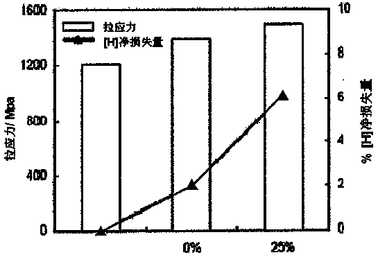
[0024] At a temperature of 500° C., a first silicon nitride film layer is first deposited on the silicon substrate. The first silicon nitride film is treated with hydrogen plasma. A second silicon nitride film layer is deposited on the first silicon nitride film layer, and the second silicon nitride film is treated with hydrogen plasma again. Afterwards, a third silicon nitride film layer is deposited on the second silicon nitride film layer, and the third silicon nitride film is treated with hydrogen plasma again. The entire deposition and processing is done in the same chamber. Finally, ultraviolet light is irradiated on the multilayer silicon nitride thin film layer, and the obtained silicon nitride thin film layer has high tensile stress.

Embodiment 2

[0026] At a temperature of 400° C., a first silicon nitride film layer is deposited on the silicon substrate. The first silicon nitride film is treated with ammonia gas plasma. A second silicon nitride thin film layer is deposited on the first silicon nitride thin film layer, and the second silicon nitride thin film is treated with ammonia gas plasma again. Afterwards, a third silicon nitride thin film layer is deposited on the second silicon nitride thin film layer, and the third silicon nitride thin film is treated with ammonia gas plasma again. Subsequently, a fourth silicon nitride thin film layer is deposited on the third silicon nitride thin film layer, and the fourth silicon nitride thin film is treated with ammonia gas plasma again. The entire deposition and processing is done in the same chamber. The deposition and processing process is repeated until the silicon nitride film reaches the desired thickness. Finally, the obtained multilayer silicon nitride thin film ...


PUM


Abstract

The invention discloses a method for manufacturing a silicon nitride film with high tensile stress, comprising the following steps of: depositing a first silicon nitride film layer on a silicon substrate, treating the first silicon nitride film by using plasma; depositing a second silicon nitride film layer on the first silicon nitride film layer, treating the second silicon nitride film by using plasma; and performing ultraviolet irradiation on the multilayer silicon nitride film. The manufacturing method provided by the invention can be used for manufacturing a silicon nitride film with the smallest stress of 1.8GPa at a lower manufacturing cost, the silicon nitride film can be applied to an NMOS(N-channel Metal Oxide Semiconductor) device for greatly increasing the electromobility, and the production process is quite simple.

Description

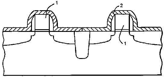
technical field [0001] The invention relates to a method for manufacturing a silicon nitride film, in particular to a method for manufacturing a silicon nitride film with high tensile stress. Background technique [0002] In the manufacture of modern CMOS devices, especially for thin-film technology below 90 nanometers (nm), many methods have been introduced to improve the electrical mobility of carriers. Among them, in the manufacturing process of NMOS devices, silicon nitride with high tensile stress is usually used as the contact etch stop layer (Contact Etch Stop Layer, CESL for short), and the stress condition in the NMOS channel is changed through its high tensile stress, thereby increase its electrical mobility. [0003] In order to obtain a silicon nitride film with higher tensile stress, plasma treatment in a nitrogen-containing environment or ultraviolet light irradiation is usually used to remove a certain amount of hydrogen in the film and shrink the film to inc...

Claims


Application Information

Patent Timeline
Patent Type & Authority Patents(China)
IPC IPC(8): H01L21/26H01L21/318H01L21/8234
Inventor 徐强张文广郑春生陈玉文
Owner SHANGHAI HUALI MICROELECTRONICS CORP
Learn More