Inverse ratio or small ratio NMOS (N-channel Metal Oxide Semiconductor) tube layout structure resistant to total dose irradiation effect

A radiation effect and anti-total dose technology, applied in the direction of electrical components, circuits, semiconductor devices, etc., can solve problems such as impracticality, application limitations, layout and wiring design limitations, etc., to achieve commercial process compatibility, small footprint, layout and wiring Convenience and flexible effects

Active Publication Date: 2012-04-11
58TH RES INST OF CETC
View PDF5 Cites 6 Cited by
  • Summary
  • Abstract
  • Description
  • Claims
  • Application Information

AI Technical Summary

Problems solved by technology

However, due to the structural limitation of the ring gate, it is only suitable for units with an NMOS transistor with a width-to-length ratio of at least 4:1.
However, the NMOS transistor with a small width-to-length ratio cannot be realized by using the ring gate layout structure. In addition, because the NMOS drain terminal is surrounded by the ring gate, the layout design is very limited.
Therefore, the application of the reinforced layout structure of the ring gate in the radiation-resistant circuit is limited.

Method used


Image

  • Inverse ratio or small ratio NMOS (N-channel Metal Oxide Semiconductor) tube layout structure resistant to total dose irradiation effect
  • Inverse ratio or small ratio NMOS (N-channel Metal Oxide Semiconductor) tube layout structure resistant to total dose irradiation effect
  • Inverse ratio or small ratio NMOS (N-channel Metal Oxide Semiconductor) tube layout structure resistant to total dose irradiation effect

Examples


Embodiment Construction

[0026] The present invention will be further described below in conjunction with specific drawings and embodiments.

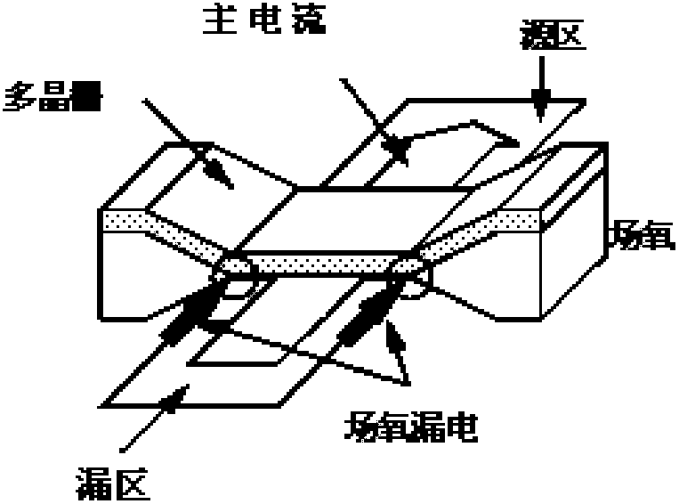
[0027] Such as figure 1 Shown: It is a conventional NMOS transistor manufactured by a self-aligned process. The polysilicon gate is deposited on a thin oxide layer, and the source / drain is formed by implanting the active area not covered by polysilicon. The circuit density produced by this process is High, but the polysilicon gate creates a parasitic transistor in the gate oxide and field-oxygen transition regions, which is very sensitive to total dose effects. Because the field oxygen and the gate oxide layer will be ionized under radiation conditions to generate electron-hole pairs; due to the trapping effect, positive charges will accumulate on the silicon dioxide side of the silicon / silicon dioxide system to form an interface state, which seriously affects to the current and voltage characteristics of transistors. As the radiation dose increases, the leak...


PUM


Abstract

The invention relates to an inverse ratio or small ratio NMOS (N-channel Metal Oxide Semiconductor) tube layout structure resistant to a total dose irradiation effect. The structure comprises a semiconductor substrate and an active region, wherein polycrystalline grids are deposited in the active region of the semiconductor substrate; a source end injection protection ring and a leakage end injection projection ring are arranged at two ends in the active region corresponding to the deposited polycrystalline grids respectively; a source end and a leakage end are formed in the source end injection protection ring and the leakage end injection protection ring respectively by performing ion injection; both the source end and the leakage end are surrounded by the polycrystalline grids; and the source end and the leakage end are isolated through the polycrystalline grids. Due to the adoption of the structure, the problem of electric leakage and isolation failure caused after field oxygen induction inversion under the radiation condition is completely solved; meanwhile, an edge parasitic transistor which is very sensitive to the total dose effect does not exist at the boundary between the polycrystalline grids and a field oxygen region, so that the aim of reinforcing the total dose is fulfilled; and an inverse ratio or small ratio reinforced NMOS tube which is difficult to realize with the conventional annular grids can be realized, the structure is simple and is compatible with the commercial process, and has a small occupied area, and layout wiring is more convenient and flexible.

Description

technical field [0001] The invention relates to a MOS tube layout structure, in particular to an inverse-proportional or small-scale NMOS tube layout structure against total dose radiation effect, belonging to the technical field of MOS tube layout. Background technique [0002] When the device is continuously exposed to ionizing radiation (such as X-rays, gamma rays, etc.), the total dose radiation effect will occur. For NMOS transistors, there is a layer of 50-200 nanometer silicon dioxide dielectric layer between the gate and the substrate. Under radiation conditions, a certain number of electron-hole pairs are generated by ionization in the silicon dioxide medium. When a forward bias is applied to the gate, most of the electrons with high mobility overflow to the gate, some electrons recombine with hole pairs, and most of the holes flow toward the SiO2 under the action of a positive electric field. 2 / Si interface, and part of it is transported by SiO at the interface ...

Claims


Application Information

Patent Timeline
Patent Type & Authority Applications(China)
IPC IPC(8): H01L29/78H01L29/06H01L29/43
Inventor 罗静徐睿邹文英薛忠杰周昕杰胡永强
Owner 58TH RES INST OF CETC
Why Eureka
Try Eureka