Epitaxial method for improving luminous efficiency of GaN-based LED (Light Emitting Diode)

A technology of luminous efficiency and epitaxial growth, applied in chemical instruments and methods, crystal growth, electrical components, etc., can solve problems such as lattice constant and thermal expansion coefficient mismatch, affecting the internal quantum efficiency of materials, etc., to reduce the impact and improve the internal The effect of quantum efficiency

Inactive Publication Date: 2012-04-18
HC SEMITEK CORP
View PDF0 Cites 9 Cited by
  • Summary
  • Abstract
  • Description
  • Claims
  • Application Information

AI Technical Summary

Problems solved by technology

[0003] At present, most GaN-based blue-green LEDs are heteroepitaxially grown on sapphire (Al2O3) substrates by metal-organic compound vapor deposition (MOCVD: Metal-Organic Chemical Vapor Deposition), but due to the gap between GaN and sapphire substrates With large lattice constant and thermal expansion coefficient mismatch, strong stress and a large number of dislocations and defects will be generated at the interface. For the current general-purpose blue-green LED epitaxial structure, such as figure 1 As shown, these dislocations and defects will extend to the surface of the epitaxial layer of the sample, with a density as high as 1×10¹⁹ / cm3, which seriously affects the internal quantum efficiency of the material

Method used


Image

  • Epitaxial method for improving luminous efficiency of GaN-based LED (Light Emitting Diode)
  • Epitaxial method for improving luminous efficiency of GaN-based LED (Light Emitting Diode)
  • Epitaxial method for improving luminous efficiency of GaN-based LED (Light Emitting Diode)

Examples


Embodiment 1

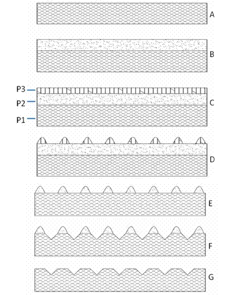
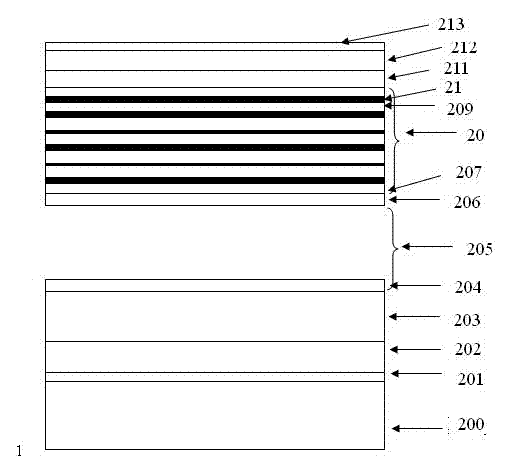
[0014] 1) Place the sapphire substrate 200 with (0001) crystal orientation on a graphite disk and send it into the reaction chamber, heat the sapphire substrate to 1060°C for 5 minutes.

[0015] 2) Lower the temperature to 540° C. to grow a low-temperature buffer layer 201 with a thickness of about 30-70 nm.

[0016] 3) Raise the temperature to 1020°C to grow a nucleation layer with a thickness of about 100-300nm.

[0017] 4) Raise the temperature to 1080° C. to grow an undoped GaN layer 202 with a thickness of about 1 μm.

[0018] 5) Growing a Si-doped nGaN layer 203 with a thickness of about 1.7um.

[0019] 6) Lower the temperature to 850° C. to grow a Si-doped n-type current spreading layer 204 with a thickness of about 40 nm.

[0020] 7) Treat the surface of the n-type current spreading layer by injecting SiH4 at 700° C. for 10 seconds 205 .

[0021] 8) Grow the nucleation layer for 20s with a growth pressure of 600Torr.

[0022] 9) Grow a Si-doped nGaN surface recover...

Embodiment 2

[0029] 15) Place the sapphire substrate with (0001) crystal orientation on a graphite disk and send it into the reaction chamber, heat the sapphire substrate to 1060°C for 5 minutes.

[0030] 16) Lower the temperature to 540°C to grow a low-temperature buffer layer with a thickness of about 30-70nm.

[0031] 17) Raise the temperature to 1020°C to grow a nucleation layer with a thickness of about 100-300nm.

[0032] 18) Raise the temperature to 1080°C to grow an undoped GaN layer about 1um thick.

[0033] 19) Grow a Si-doped nGaN layer about 1.7um thick.

[0034] 20) Lower the temperature to 850°C to grow a Si-doped n-type current spreading layer with a thickness of about 40nm.

[0035] 21) Heat up to 900°C and pass H2 for 10 minutes to treat the surface of the n-type current spreading layer.

[0036] 22) Grow the nucleation layer for 20s with a growth pressure of 600Torr.

[0037] 23) Grow a Si-doped nGaN layer with a thickness of about 50?, and the growth pressure is 100T...

Embodiment 3

[0044] 29) Place the sapphire substrate with (0001) crystal orientation on a graphite disk and send it into the reaction chamber, heat the sapphire substrate to 1060°C for 5 minutes.

[0045] 30) Lower the temperature to 540°C to grow a low-temperature buffer layer with a thickness of about 30-70nm.

[0046] 31) Raise the temperature to 1020°C to grow a nucleation layer with a thickness of about 100-300nm.

[0047] 32) Raise the temperature to 1080°C to grow an undoped GaN layer about 1um thick.

[0048] 33) Grow a Si-doped nGaN layer about 1.7um thick.

[0049] 34) Lower the temperature to 850°C to grow a Si-doped n-type current spreading layer with a thickness of about 40nm.

[0050] 35) Raise the temperature to 1100°C and pass CH4 for 20 minutes to treat the surface of the n-type current spreading layer.

[0051] 36) Grow the nucleation layer for 20s, and the growth pressure is 600Torr.

[0052] 37) Grow a Si-doped nGaN surface recovery layer about 50? thick with a grow...


PUM


Abstract

The invention discloses an epitaxial growth method for improving the luminous efficiency of a GaN-based LED (Light Emitting Diode). The epitaxial growth method comprises the following steps of: adding a surface treating procedure between an n-type current diffusion layer and an n-type space layer on the basis of a buffer layer, a uGaN layer, an nGaN layer, an n-type current expansion layer, the n-type space layer, a quantum well active region, a p-type electronic blocking layer, a p-type GaN layer and a contact layer on a substrate of a traditional GaN-based LED structure; damaging and releasing the defect and the stress extending from the interface of the substrate and the GaN to the current diffusion layer; recovering the surface of a material to be flat by controlling growing conditions; and growing the quantum well active region. The result shows that a grown quantum well is less influenced by the defect and the stress compared with a traditional growing technology, so that the luminous intensity of a sample can be effectively improved. The epitaxial growth method disclosed by the invention is suitable for epitaxial growth of the GaN-based LED in a blue-green light waveband.

Description

technical field [0001] The invention relates to the epitaxial growth of GaN-based materials, in particular to the epitaxial growth of GaN-based blue-green light emitting diodes. Background technique [0002] Light Emitting Diode (LED, Light Emitting Diode) has the advantages of longevity, energy saving, environmental protection, and high reliability. In recent years, LED has played an increasingly important role in large-screen color displays, traffic lights, and lighting. However, in order to play a greater role in the field of full-color display and lighting, the brightness of LEDs needs to be further improved. [0003] At present, most GaN-based blue-green LEDs are heteroepitaxially grown on sapphire (Al2O3) substrates by metal-organic compound vapor deposition (MOCVD: Metal-Organic Chemical Vapor Deposition), but due to the gap between GaN and sapphire substrates With large lattice constant and thermal expansion coefficient mismatch, strong stress and a large number of ...

Claims


Application Information

Patent Timeline
IPC IPC(8): C30B29/38C30B25/02H01L33/00
Inventor 孙玉芹王江波魏世祯刘榕
Owner HC SEMITEK CORP
Why Eureka
Try Eureka