
Patsnap Eureka
For R&D, Patsnap Eureka makes reading and utilizing patents & technical documents easy.
Patsnap Eureka AIR
Designed for self-driven R&D workflows. Generate viable solutions, solve complex R&D challenges, empower your innovation with AI.

Patsnap Eureka Materials
Designed for material experts only. Revolutionize your material R&D, from search, analyze, to developing new materials.

TechResearch
Generate reliable direction feasibility study reports for your R&D in just a few steps.

TechSeek
Discover and master advanced knowledge NOW. Basics, ideas, possibilities, all at once.

TechMind
As an expert in R&D Theories, TechMind can generates customized viable solutions instantly.

TechRisk
Analyze your overall solution with one click, know your potential R&D risks in advance.

TechMonitor
Get weekly tech updates, stay abreast of the latest tech innovations and key insights.
Coupling waveguide, manufacture method thereof and semiconductor photoelectronic device applying coupling waveguide
A technology for optoelectronic devices and coupling waveguides, applied in the structure of optical waveguide semiconductors, optical waveguides and optical components, etc., can solve problems such as disadvantage, small driving voltage, weak light absorption at the back end of the waveguide, etc., to improve absorption efficiency, prevent The effect of increasing the driving voltage and preventing excessive photo-generated carriers
- Summary
- Abstract
- Description
- Claims
- Application Information
AI Technical Summary
Problems solved by technology
Method used
Image

Examples
Embodiment 1
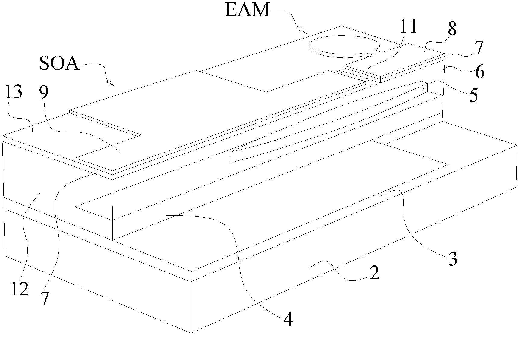
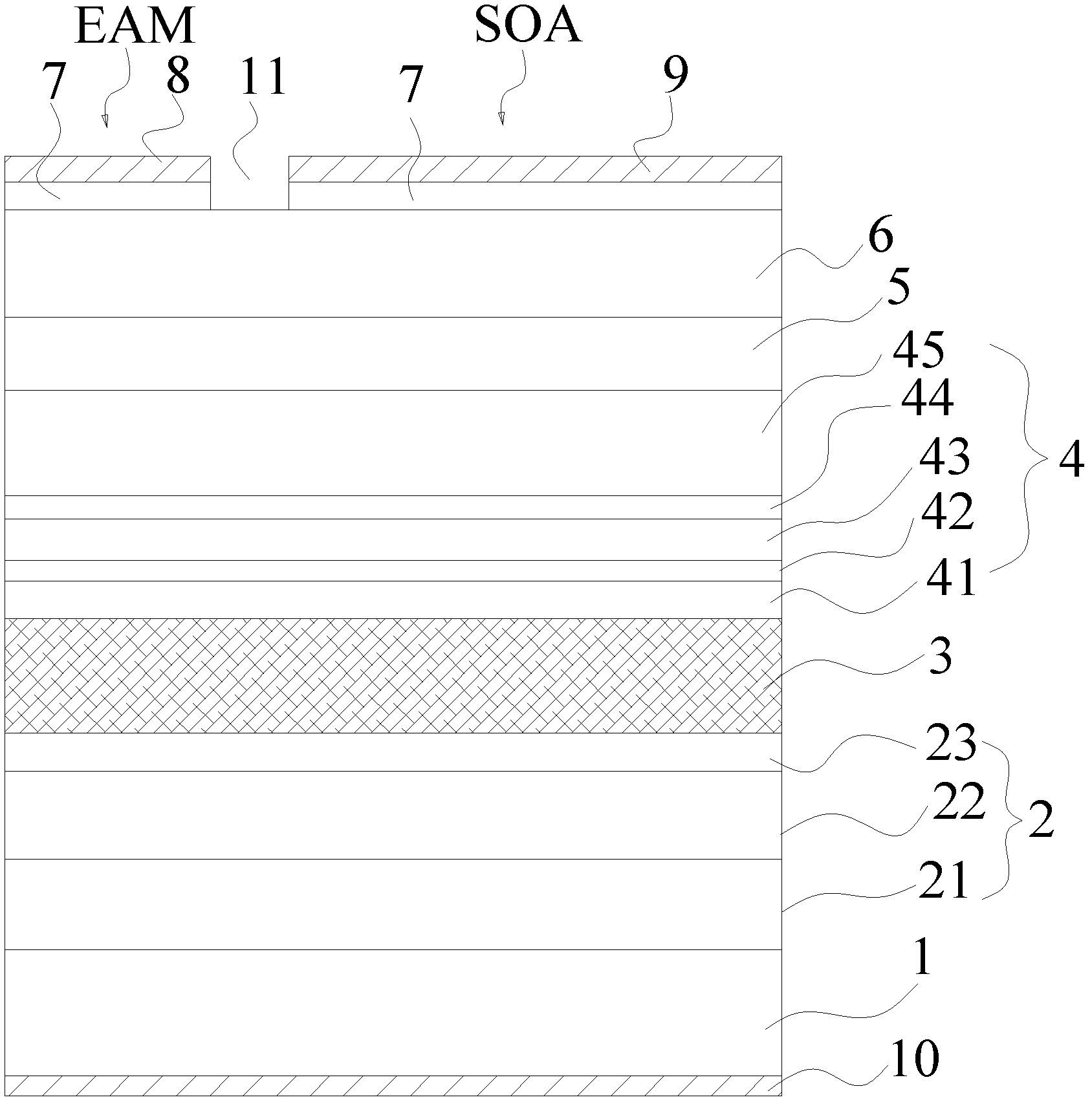
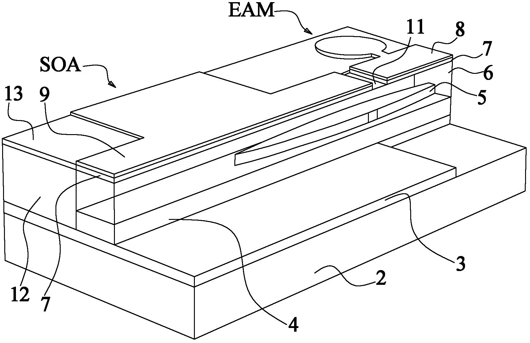
[0034] like figure 1 As shown, the coupling waveguide of this embodiment includes substrates 1 distributed sequentially from bottom to top (substrate 1 is in figure 1 not shown in), the lower waveguide cladding layer 2, the first waveguide core layer 3, the isolation layer 4, the second waveguide core layer 5 and the upper waveguide cladding layer 6, the first waveguide core layer 3 is an active waveguide layer, The second waveguide core layer 5 is a coupling and guiding waveguide layer, the second waveguide core layer 5 has a width gradient section whose lateral width gradually changes along the light guiding direction, and the upper waveguide cladding layer 6 covers the second waveguide core layer 5. The top and sides of the waveguide core layer 5.
[0035] In this embodiment, the lateral width of the width gradient section of the second waveguide core layer 5 first gradually becomes wider and then gradually narrows along the light guiding direction. In other embodiments o...
Embodiment 2
[0039] A method of manufacturing the above coupling waveguide, comprising the following steps:
[0040] S1: Epitaxial growth of the lower waveguide cladding layer 2, the first waveguide core layer 3, the isolation layer 4 and the second waveguide core layer 5 in sequence on a clean epitaxial wafer;
[0041] S2: Processing the second waveguide core layer 5 to form a width gradient section whose lateral width changes along the light guiding direction;
[0042] S3: performing secondary epitaxy to form an upper waveguide cladding layer 6 covering the upper side and side surfaces of the second waveguide core layer 5 .
[0043] In this embodiment, the step of processing the second waveguide core layer 5 includes using electron beam exposure to make a mask on the second waveguide core layer 5, and then performing dry etching first and then wet etching The process of the second waveguide core layer 5. In other embodiments, other methods may also be used to change the lateral width o...
Embodiment 3
[0046] like figure 1 As shown, a semiconductor optoelectronic device having the coupling waveguide described in Embodiment 1, the semiconductor optoelectronic device includes an electro-absorption modulator EAM, and the second waveguide core layer 5 of the coupling waveguide corresponds to the electro-absorption modulator EAM The lateral width of the portion is gradually narrowed along the light guiding direction.
[0047] The semiconductor optoelectronic device also includes a semiconductor optical amplifier SOA sharing the same coupling waveguide with the electro-absorption modulator EAM, and the second waveguide core layer 5 of the coupling waveguide is along the guideway along the lateral width of the corresponding part of the semiconductor optical amplifier SOA. The light direction gradually widens.
[0048] The semiconductor optical amplifier SOA and the electro-absorption modulator EAM are successively arranged adjacent to each other along the light guiding direction, ...
PUM
 Abstract
Description
Claims
Application Information
 - R&D Engineer
- R&D Manager
- IP Professional
- Industry Leading Data Capabilities
- Powerful AI technology
- Patent DNA Extraction
Browse by: Latest US Patents, China's latest patents, Technical Efficacy Thesaurus, Application Domain, Technology Topic, Popular Technical Reports.
© 2024 PatSnap. All rights reserved.Legal|Privacy policy|Modern Slavery Act Transparency Statement|Sitemap|About US| Contact US: help@patsnap.com