


Quick Research
Generate reliable direction feasibility study reports for your R&D in just a few steps.

Technical Q&A
Discover and master advanced knowledge NOW. Basics, ideas, possibilities, all at once.

Find Solutions
As an expert in R&D theories, this can generate solutions to your technical problems instantly.

Evaluate Feasibility
Analyze your overall solution with one click, know your potential R&D risks in advance.

Monitor Landscape
Get weekly tech updates, stay abreast of the latest tech innovations and key insights.
Coupling waveguide, manufacture method thereof and semiconductor photoelectronic device applying coupling waveguide
A technology of optoelectronic devices and coupling waveguides, applied in the structure of optical waveguide semiconductors, optical waveguides, optical components, etc., can solve the problems of weak light absorption, small driving voltage, and disadvantages at the back end of waveguides, and prevent photogenerated carriers Excessive, the effect of preventing the drive voltage from increasing and improving the absorption efficiency
- Summary
- Abstract
- Description
- Claims
- Application Information
AI Technical Summary
Problems solved by technology
Method used
Image

Examples
Embodiment 1
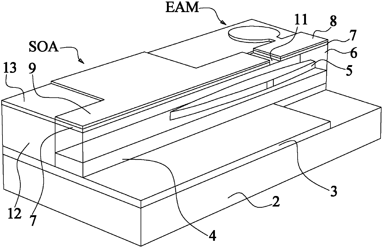
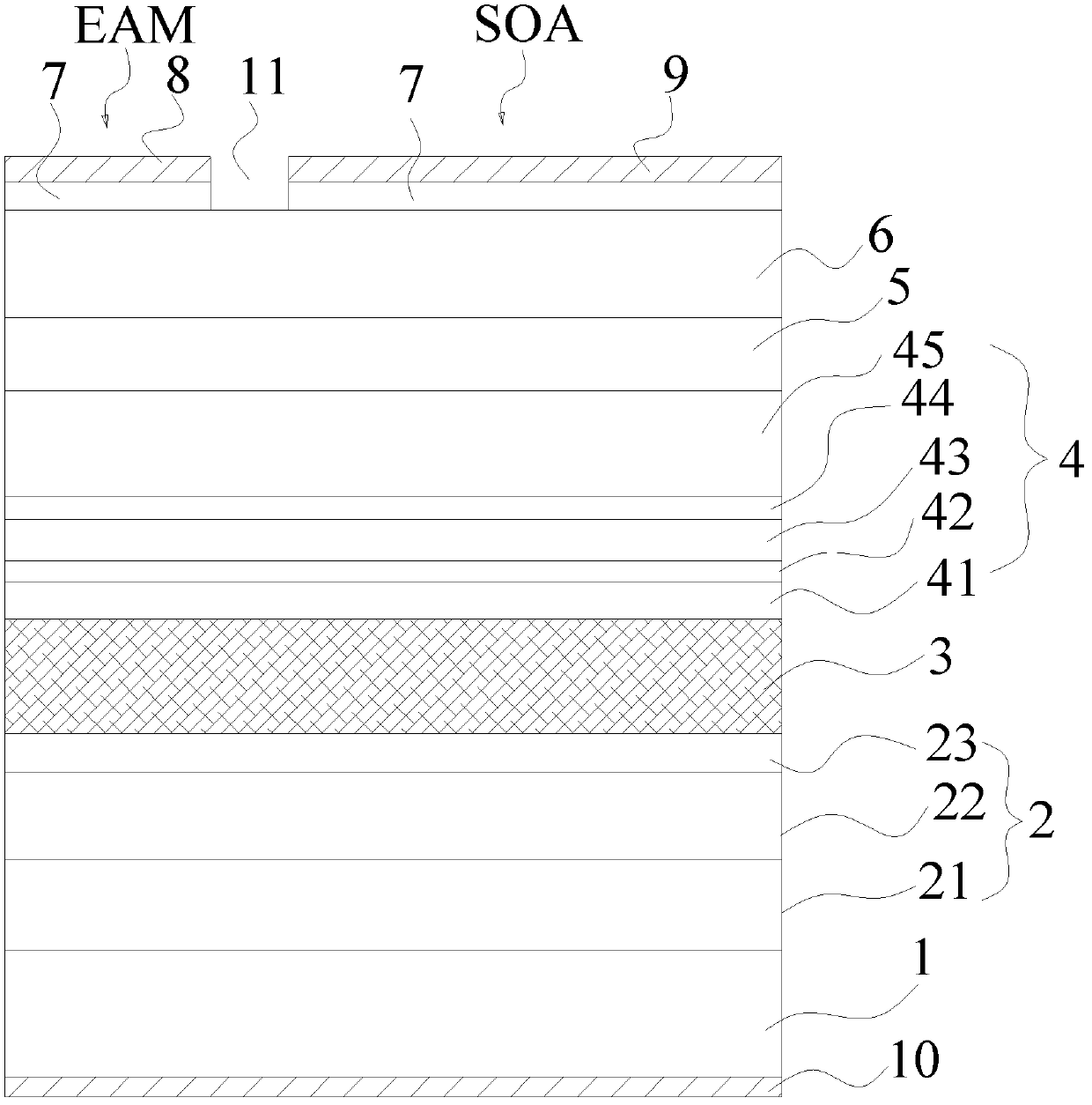
[0034] Such as figure 1 As shown, the coupled waveguide of this embodiment includes a substrate 1 distributed in order from bottom to top (the substrate 1 is figure 1 Not shown), the lower waveguide cladding layer 2, the first waveguide core layer 3, the isolation layer 4, the second waveguide core layer 5 and the upper waveguide cladding layer 6, the first waveguide core layer 3 is an active waveguide layer, The second waveguide core layer 5 is a coupling guiding waveguide layer, the second waveguide core layer 5 has a width gradient section with a lateral width gradually changing along the light guiding direction, and the upper waveguide cladding layer 6 covers the second waveguide layer. The top and side of the waveguide core 5.
[0035] In this embodiment, the lateral width of the tapered width section of the second waveguide core layer 5 first gradually widens and then gradually narrows along the light guiding direction. In other embodiments of the present invention, accordi...
Embodiment 2
[0039] A method for manufacturing the above-mentioned coupled waveguide includes the following steps:
[0040] S1: The lower waveguide cladding layer 2, the first waveguide core layer 3, the isolation layer 4, and the second waveguide core layer 5 are sequentially grown on a clean epitaxial wafer at one time;
[0041] S2: processing the second waveguide core layer 5 to form a gradual width section whose lateral width changes along the light guiding direction;
[0042] S3: Perform secondary epitaxy to form an upper waveguide cladding layer 6 covering the upper and side surfaces of the second waveguide core layer 5.
[0043] In this embodiment, the step of processing the second waveguide core layer 5 includes using electron beam exposure to make a mask on the second waveguide core layer 5, and then dry etching first, and then wet etching. The process of the second waveguide core 5. In other embodiments, other methods may be used to change the lateral width of the second waveguide core ...
Embodiment 3
[0046] Such as figure 1 As shown, a semiconductor optoelectronic device having the coupled waveguide described in Embodiment 1, the semiconductor optoelectronic device includes an electro-absorption modulator EAM, and the second waveguide core layer 5 of the coupled waveguide corresponds to the electro-absorption modulator EAM The lateral width of the part gradually narrows along the light guide direction.
[0047] The semiconductor optoelectronic device also includes a semiconductor optical amplifier SOA that shares the same coupling waveguide with the electro-absorption modulator EAM. The second waveguide core layer 5 of the coupling waveguide and the corresponding portion of the semiconductor optical amplifier SOA have a lateral width along the guide The light direction gradually widens.
[0048] The semiconductor optical amplifier SOA and the electro-absorption modulator EAM are arranged adjacent to each other along the light guiding direction, and the lateral width of the seco...
PUM
 Abstract
Description
Claims
Application Information
 - R&D Engineer
- R&D Manager
- IP Professional
- Industry Leading Data Capabilities
- Powerful AI technology
- Patent DNA Extraction
Browse by: Latest US Patents, China's latest patents, Technical Efficacy Thesaurus, Application Domain, Technology Topic, Popular Technical Reports.
© 2024 PatSnap. All rights reserved.Legal|Privacy policy|Modern Slavery Act Transparency Statement|Sitemap|About US| Contact US: help@patsnap.com