Under-gate technology CMOS (complementary metal oxide semiconductor) device for inhibiting drain induction barrier lower effect and preparation method thereof

A gate-last process and inductive barrier technology are applied in the field of gate-last process CMOS devices to achieve the effects of low implementation cost, improved performance and simple process flow

Active Publication Date: 2012-04-18
SHANGHAI HUALI MICROELECTRONICS CORP
View PDF5 Cites 3 Cited by
  • Summary
  • Abstract
  • Description
  • Claims
  • Application Information

AI Technical Summary

Problems solved by technology

[0007] The invention provides a gate-last process CMOS device that suppresses the effect of drain-induced barrier lowering. It aims at the existing deficiency of suppressing the DIBL effect, and locally changes the work of the gate by implanting ions into the semiconductor gate close to the drain. Function, so as to achieve the purpose of suppressing the DIBL effect, and will not cause an additional increase in the leakage current of the drain PN junction

Method used


Image

  • Under-gate technology CMOS (complementary metal oxide semiconductor) device for inhibiting drain induction barrier lower effect and preparation method thereof
  • Under-gate technology CMOS (complementary metal oxide semiconductor) device for inhibiting drain induction barrier lower effect and preparation method thereof
  • Under-gate technology CMOS (complementary metal oxide semiconductor) device for inhibiting drain induction barrier lower effect and preparation method thereof

Examples


Embodiment 1

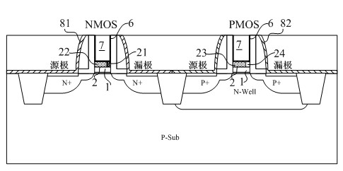
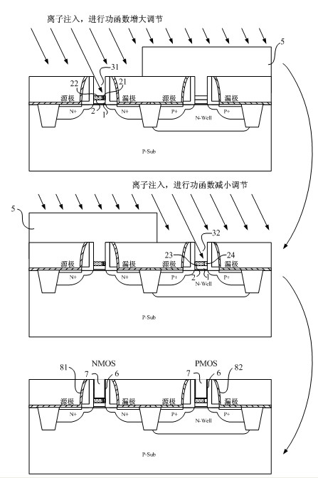
[0047] Such as figure 1 As shown, the present invention provides a gate-last process CMOS device that suppresses the drain-induced barrier lowering effect, and the gate-last process CMOS device includes an N-type MOS transistor and a P-type MOS transistor. In the gates of the N-type MOS transistor and the P-type MOS transistor, a high dielectric layer 1 and a metal oxide dielectric material layer 2 covering the high dielectric layer 1 are included, and the high dielectric Below layer 1 may also include optionally growing a thin oxide layer.

[0048] Wherein, in the metal oxide dielectric material layer 2 of the N-type MOS transistor, ions with a large work function are implanted into the part 21 close to the drain terminal, which improves the performance of the metal oxide dielectric material layer 2 close to the drain terminal. The work function of part 21 increases the flat-band voltage required by the gate at the drain terminal during use, so that in its channel, the elect...

Embodiment 2

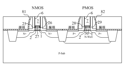
[0063] Such as figure 2 As shown, the difference between the CMOS structure of this embodiment and the above-mentioned embodiment 1 is that,

[0064] In this embodiment, the metal oxide dielectric material layer 2 in the gate groove 31 of the N-type MOS transistor is implanted with ions having a large work function near the source end portion 25 and the drain end portion 26, thereby improving the dielectric strength. The work function of the electrical material near the source terminal portion 25 and the drain terminal portion 26 makes the work function of both of them greater than the work function of the middle portion 27 between the drain terminal and the source terminal. In this way, the flat-band voltage required by the gate at the drain terminal and the source terminal can be increased, and in its channel, the electronic potential barrier close to the source and drain terminals can be increased at the same time, thereby effectively suppressing the N-type semiconductor d...


PUM


Abstract

The invention provides an under-gate technology CMOS (complementary metal oxide semiconductor) device for inhibiting drain induction barrier reduction effect and a preparation method thereof. The CMOS device comprises an N-type MOS (metal oxide semiconductor) transistor and a P-type MOS (metal oxide semiconductor) transistor, wherein gate grooves of N-type MOS transistor gate and a P-type MOS transistor gate comprise a metal oxide dielectric material layer respectively; ions with different work functions are injected to the metal oxide dielectric material layer, so that the work functions of the N-type MOS transistor gate close to a drain end or two ends of a drain and a source are increased, and the work functions of the P-type MOS transistor gate close to the drain end or close to two ends of the drain and the source are decreased, thus the drain induction barrier lower effect of the CMOS device is inhibited. According to the invention, leakage current of a PN junction at the drain end can not be caused while changing the working functions of the drain end of the CMOS device or the working functions close to two ends of the drain or source so as to inhibit DIBL (drain induction barrier lower) effect effectively, thus the performances of a semiconductor chip are improved effectively; and the method has simple process flow, low implementation cost and no additional cost burden.

Description

technical field [0001] The invention relates to an integrated circuit manufacturing method, in particular to a gate-last process CMOS device which suppresses the effect of lowering the drain induction potential barrier. Background technique [0002] Drain induction barrier lower (DIBL) effect is an undesirable phenomenon that occurs in small-sized field effect transistors (FETs) in the semiconductor manufacturing process, that is, when the channel length is reduced, the drain region source The interval voltage (Vds) increases, so that when the depletion layer of the drain junction and the source junction is close, the electric force line in the channel can cross from the drain region to the source region, and cause the barrier height of the source terminal to decrease, so that the source region is injected into the channel The number of carriers increases, resulting in an increase in drain current. And when the channel length is shorter, the DIBL effect is more serious. ...

Claims


Application Information

Patent Timeline
Patent Type & Authority Applications(China)
IPC IPC(8): H01L27/092H01L29/423H01L21/8238H01L21/28
Inventor 黄晓橹谢欣云陈玉文邱慈云
Owner SHANGHAI HUALI MICROELECTRONICS CORP
Why Eureka
Try Eureka