Check patentability & draft patents in minutes with Patsnap Eureka AI!

Photoresistance removing method

A photoresist removal and photoresist layer technology, applied in photosensitive material processing, electrical components, semiconductor/solid-state device manufacturing, etc. The effect of removing photoresist and improving product yield

Inactive Publication Date: 2012-04-25
SHANGHAI HUAHONG GRACE SEMICON MFG CORP
View PDF7 Cites 2 Cited by
  • Summary
  • Abstract
  • Description
  • Claims
  • Application Information

AI Technical Summary

Problems solved by technology

However, the inventors have found in long-term production practice that when dry etching is used to remove the photoresist layer, since the oxygen in dry etching easily reacts with the metal on the surface, such as TiN, it is difficult to form on the surface of the MIM capacitor. The etched oxide affects the subsequent process; moreover, the general dry etching usually cannot remove the photoresist layer on the surface, resulting in a decline in product yield

Method used


Image

  • Photoresistance removing method
  • Photoresistance removing method
  • Photoresistance removing method

Examples


Embodiment Construction

[0016] The photoresist removal method of the present invention will be described in detail below in conjunction with specific embodiments and accompanying drawings.

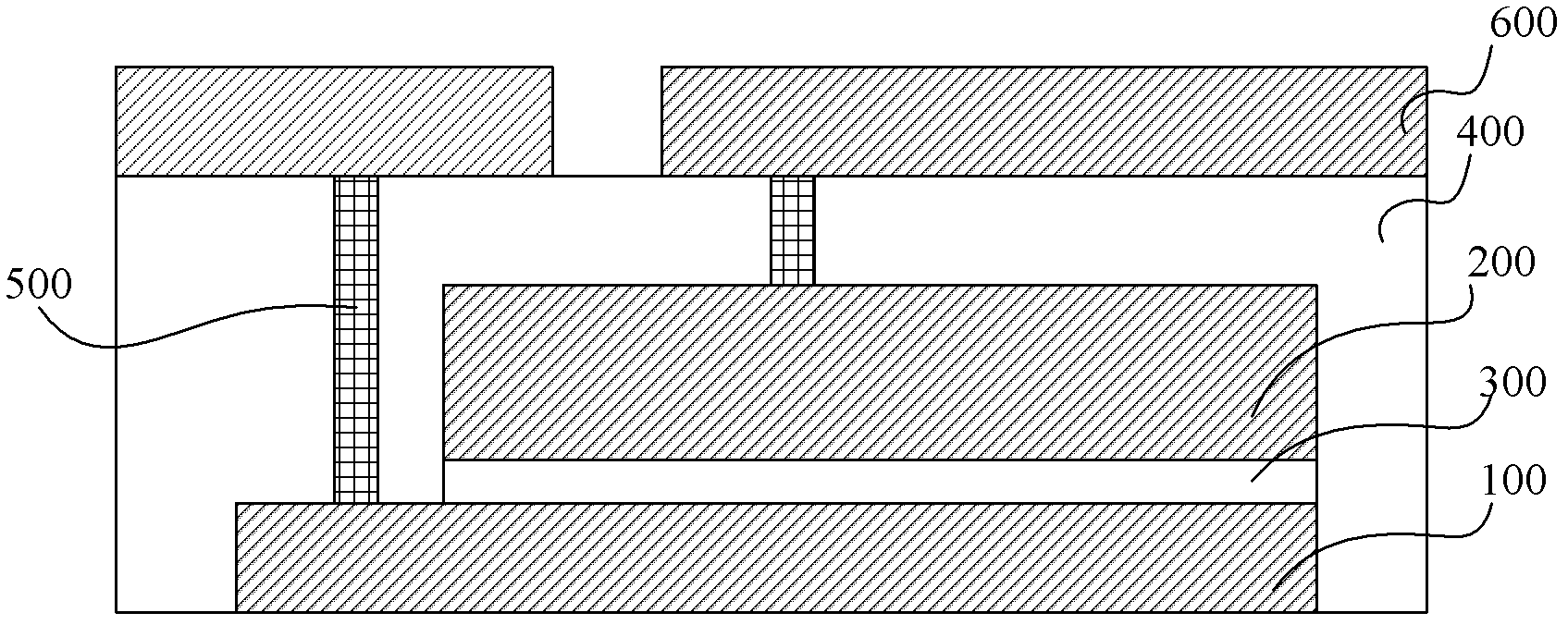
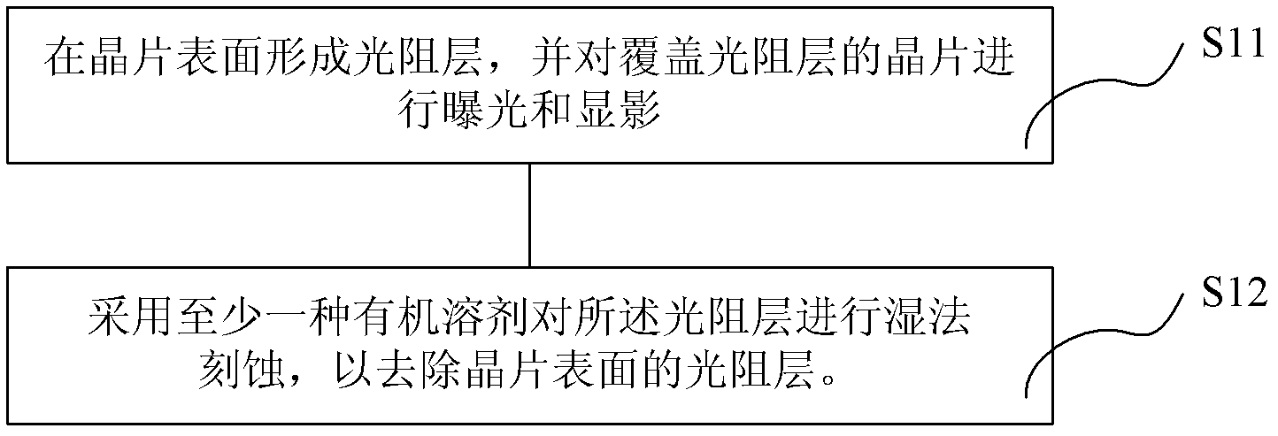
[0017] refer to figure 2 A specific implementation of the photoresist removal method of the present invention is applied to the MIM capacitor manufacturing process, and the specific implementation of the photoresist removal method may include the following steps:

[0018] Step S11, forming a photoresist layer on the surface of the wafer, and exposing and developing the wafer covered with the photoresist layer;

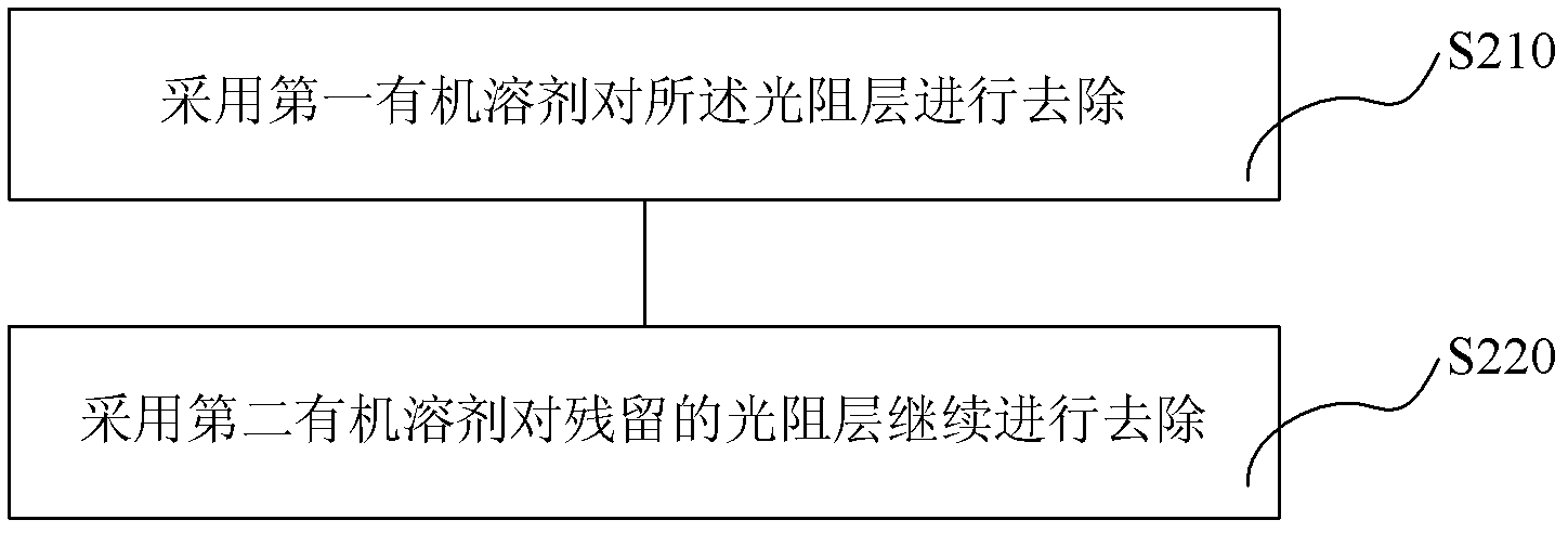
[0019] Step S12 , when the formed photoresist layer needs to be removed, at least one organic solvent is used to perform wet etching on the photoresist layer, so as to remove the photoresist layer on the surface of the wafer.

[0020] Wherein, step S11 may adopt existing process steps and parameters, and its specific implementation process does not affect the idea of ​​the present invention.

[0021] W...


PUM


Abstract

A photoresistance removing method is applied to a MIM (Metal-Insulator-Metal) capacitor manufacturing technique. The photoresistance removing method comprises the following steps of: forming a photoresistance layer on the surface of a wafer, and carrying out exposure and development on the wafer coated with the photoresistance layer; when the photoresistance layer is needed to be removed, carrying out wet process etching on the photoresistance layer by adopting at least one organic solvent so as to remove the photoresistance layer on the surface of the wafer. According to the photoresistance removing method of the invention, a step of removing photoresistance by adopting dry etching in the traditional process is changed, oxide which is difficult to etch is prevented from forming on the surface of products, and in addition, the photoresistance can be more effectively removed, thereby the yield of the products is increased.

Description

technical field [0001] The invention relates to a capacitor manufacturing process, and in particular to a photoresist removal method in the capacitor manufacturing process. Background technique [0002] Capacitive components are often used as electronic passive devices in integrated circuits such as radio frequency and monolithic microwave ICs. Common capacitor structures include metal oxide semiconductor (MOS) capacitors, PN junction capacitors, and metal-insulator-metal (MIM) capacitors. Among them, since MOS capacitors and PN junction capacitors are limited by their own structures, they are prone to generate hole layers during operation, resulting in lower frequency characteristics, while MIM capacitors can provide better frequency and temperature characteristics, so MIM capacitors can In some special applications, it provides better electrical characteristics due to MOS capacitance and PN junction capacitance. In addition, the MIM capacitor can be formed in the metal i...

Claims


Application Information

Patent Timeline
IPC IPC(8): H01L21/311H01L21/02G03F7/42
Inventor 简中祥贾敏孔秋东陈蕾
Owner SHANGHAI HUAHONG GRACE SEMICON MFG CORP
Features
  • R&D
  • Intellectual Property
  • Life Sciences
  • Materials
  • Tech Scout
  • Unparalleled Data Quality
  • Higher Quality Content
  • 60% Fewer Hallucinations
Learn More