Manufacturing process of HDI (High Density Interconnection) board

A process and circuit board technology, applied in the field of HDI board production process, can solve problems such as hidden quality problems, increase production process and production cycle, circuit board deformation, etc., to achieve good dimensional stability, shorten production cycle, and reduce production costs. Effect

Inactive Publication Date: 2012-04-25
SHENZHEN SUNTAK MULTILAYER PCB
View PDF7 Cites 21 Cited by
  • Summary
  • Abstract
  • Description
  • Claims
  • Application Information

AI Technical Summary

Problems solved by technology

[0004] However, due to the continuous improvement of customers' requirements for the reliability of laser blind vias, the outer laser blind vias are required to be completely filled or the filling degree is greater than 85%, resulting in the need for separate production of blind via filling and circuit graphics, which increases the production process. And the production cycle; and after filling the holes, it is necessary to grind the board with an abrasive belt, which is easy to deform the circuit board and bring quality hazards to the subsequent process

Method used


Image

  • Manufacturing process of HDI (High Density Interconnection) board
  • Manufacturing process of HDI (High Density Interconnection) board
  • Manufacturing process of HDI (High Density Interconnection) board

Examples


Embodiment Construction

[0021] In order to illustrate the idea and purpose of the present invention, the present invention will be further described below in conjunction with the accompanying drawings and specific embodiments.

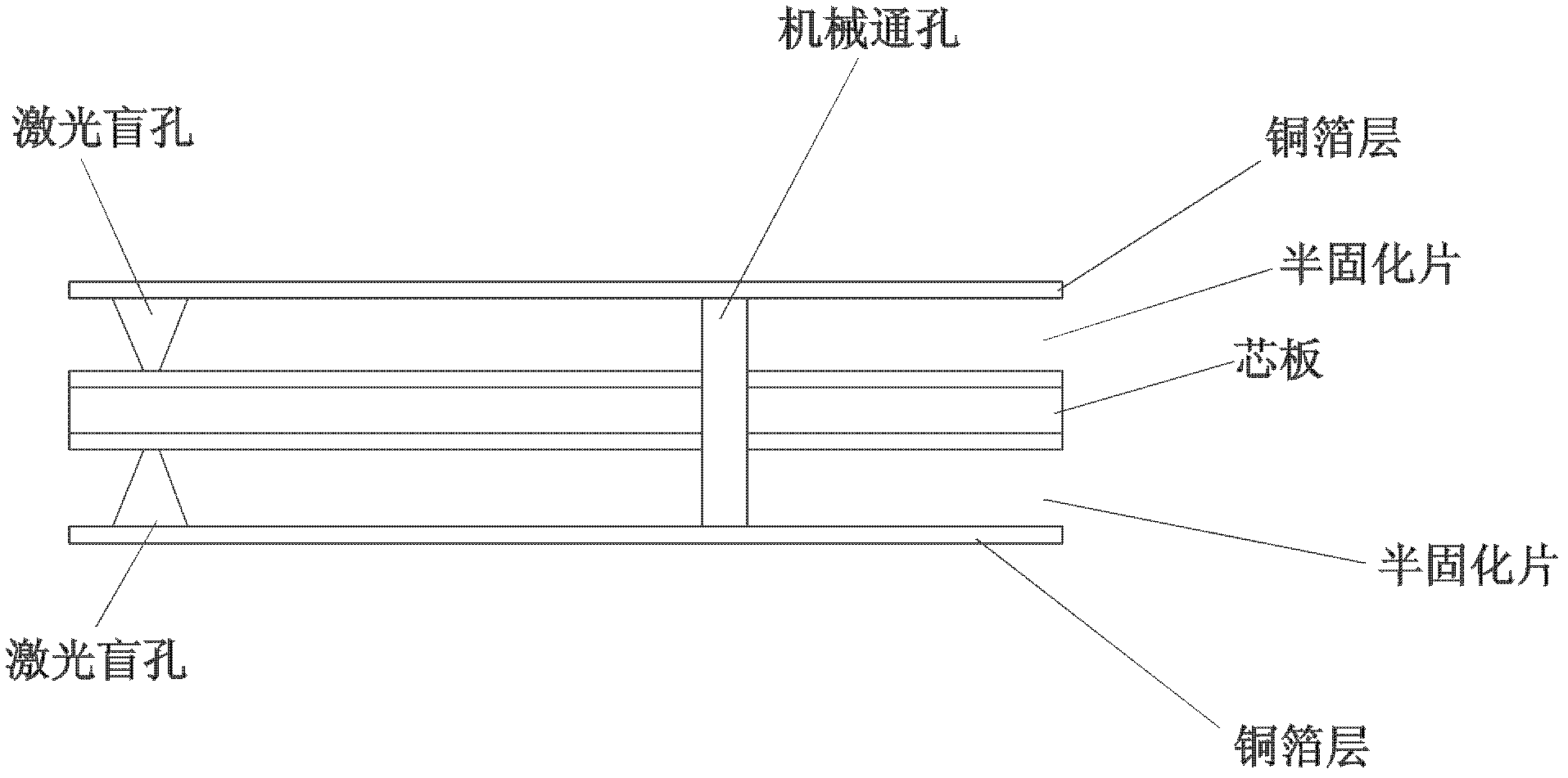
[0022] The present invention provides a production process of HDI boards, which is mainly used to solve the problems caused by many production processes due to the requirement that the outer laser blind holes are completely filled or the filling degree is greater than 85% in the current production process of HDI boards. The problem of long production cycle.

[0023] Such as figure 1 , figure 2 As shown, what the present invention provides is a kind of manufacturing process of HDI plate, comprises steps:

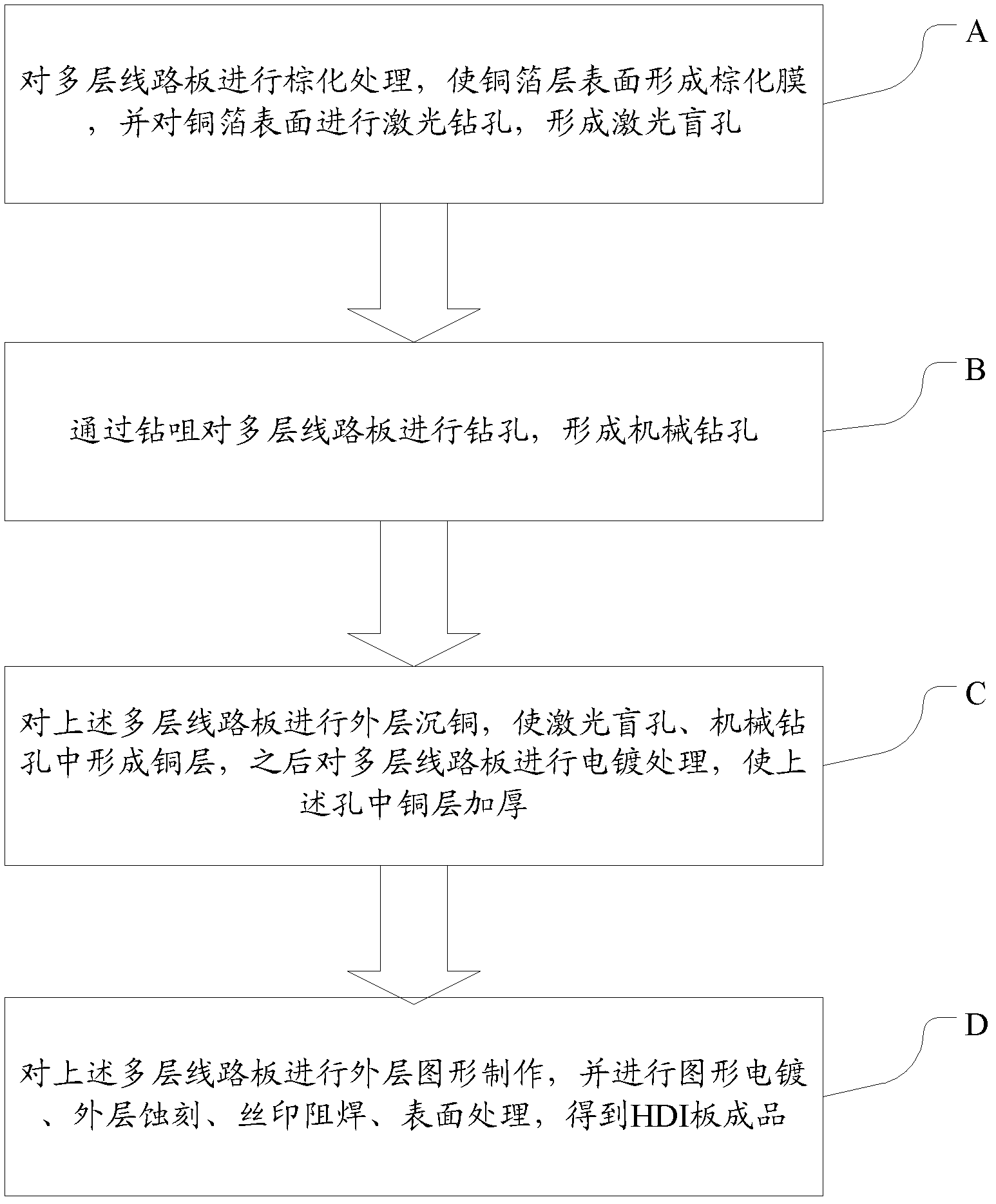
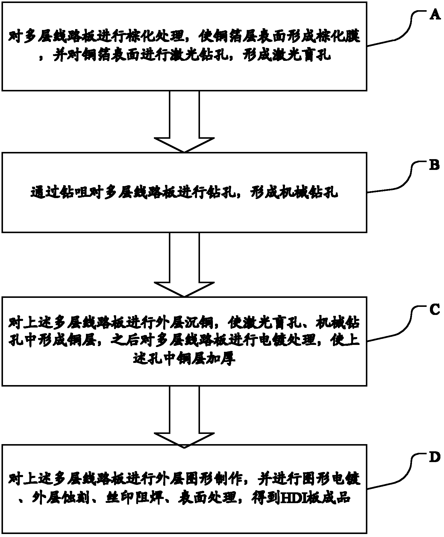
[0024] A. Carry out browning treatment on the multilayer circuit board to form a browning film on the surface of the copper foil layer, and perform laser drilling on the surface of the copper foil to form laser blind holes;

[0025] Wherein before step A includes:

[00...


PUM

PropertyMeasurementUnit
pore sizeaaaaaaaaaa

Abstract

The invention relates to a manufacturing process of an HDI (High Density Interconnection) board. The manufacturing process comprises the following steps of: A, carrying out browning treatment on a multilayer circuit board so that a browned film is formed on the surface of a copper foil layer, and carrying out laser hole drilling on the surface of the copper foil to form laser blind holes; B, carrying out hole drilling on the multilayer circuit board through a drill bit to form mechanical drill holes; C, carrying out outer-layer copper precipitation on the multilayer circuit board so that copper layers are formed in the laser blind holes and the mechanical drill holes, and carrying out electroplating treatment on the multilayer circuit board, so that the copper coppers in the laser blind holes and the mechanical drill holes are thickened; and D, carrying out outer-layer pattern making on the multilayer circuit board, and carrying out pattern electroplating, outer-layer etching, silk-screen mask soldering and surface treatment to obtain the HDI board as a finished product. Compared with the prior art, the manufacturing process disclosed by the invention has the advantages of avoiding processes, such as outer-layer copper precipitation, board electroplating, outer-layer pattern hole-electroplating, porefilling electroplating, mold stripping, board grinding with an abrasive belt and the like which are adopted after laser hole drilling, greatly shortening production cycle and reducing production cost; meanwhile, according to the manufacturing process disclosed by the invention, because the process of grinding the board with the abrasive belt is not required, size stability of the circuit board is relatively better, and the circuit board cannot deform.

Description

Technical field: [0001] The invention belongs to the technical field of circuit board production, and in particular relates to a production process of an HDI board. Background technique: [0002] HDI circuit board is also called high-density interconnection board, which means that the aperture is below 6mil, the ring diameter of the ring (Hole Pad) is below 0.25mm, the contact density is above 130 points / square, and the line width / spacing is below 3mil / 3mil printed circuit board. HDI circuit boards can reduce the production cost of multi-layer PCB boards, increase circuit density, and have the advantages of high reliability and good electrical performance. [0003] At present, the production process of HDI circuit boards is: material cutting---inner layer graphics---inner layer etching---inner layer AOI---browning---lamination---browning 2--laser drilling --Browning layer--Copper sinking on the outer layer, board electrical --- Plating hole pattern on the outer layer --- F...

Claims


Application Information

Patent Timeline
Patent Type & Authority Applications(China)
IPC IPC(8): H05K3/46
Inventor 黄海蛟杜明星翟青霞林楠白亚旭
Owner SHENZHEN SUNTAK MULTILAYER PCB
Why Eureka
Try Eureka