Device for debugging wafer-level test scheme under final test environment of automatic test device

A technology of automatic test device and test scheme, which is applied in the semiconductor field, can solve the problems of time-consuming and difficult to provide probe cards, etc., and achieve the effect of simple structure, convenient development and debugging, and short debugging time period

Active Publication Date: 2012-05-02
上海捷策创电子科技有限公司
View PDF5 Cites 7 Cited by
  • Summary
  • Abstract
  • Description
  • Claims
  • Application Information

AI Technical Summary

Problems solved by technology

It is difficult for probe cards to provide debugging methods such as signal monitoring, so engineers spend a lot of time setting up wafers (wafers) and probe stations, and it also takes a lot of money to make the results of wafer testing consistent with the results of final testing (FT) In the current period when speed to market is critical, how to quickly complete wafer-level program development and testing has become an urgent problem to be solved in the field of integrated circuit technology

Method used


Image

  • Device for debugging wafer-level test scheme under final test environment of automatic test device
  • Device for debugging wafer-level test scheme under final test environment of automatic test device
  • Device for debugging wafer-level test scheme under final test environment of automatic test device

Examples


Embodiment Construction

[0037] In order to make the technical means, creative features, objectives and effects achieved by the present invention easy to understand, the present invention will be further elaborated below.

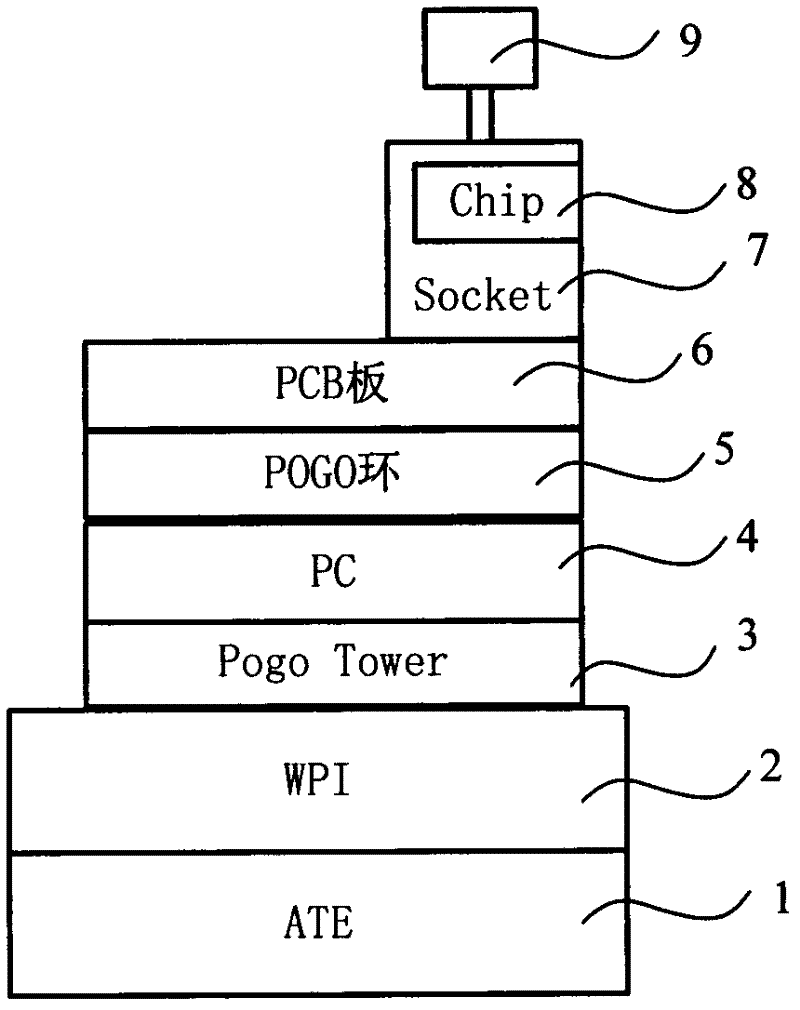
[0038] Figure 1 to Figure 7 A schematic structural view of the testing device of the present invention is shown. The test device consists of the following parts from bottom to top:

[0039] Automatic Test Equipment (ATE)1,

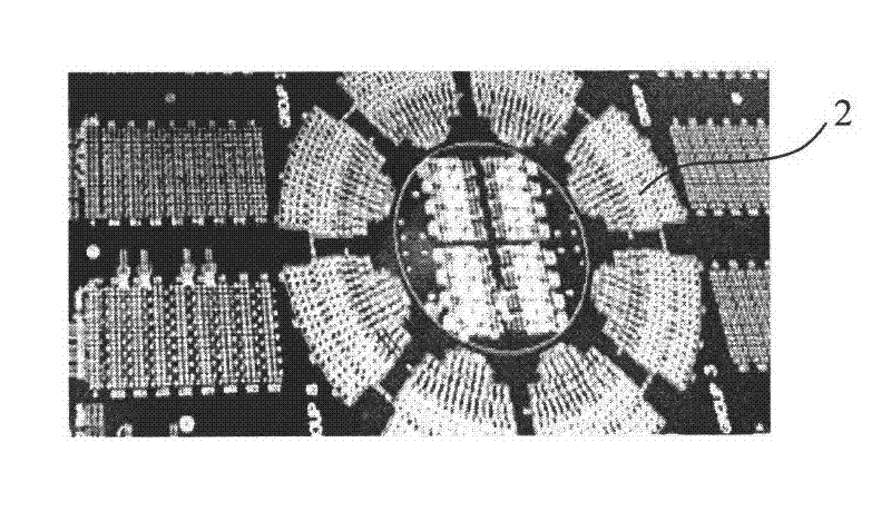
[0040] Chip test board 2 (Wafer Prober Interface, hereinafter referred to as WPI board); installed on the ATE1, figure 2 for the schematic diagram.

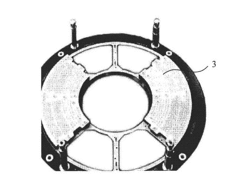
[0041] Test pogo pin ring 3 (hereinafter referred to as Pogo Tower), installed on the WPI board 2; image 3 for the schematic diagram.

[0042] Probe Card 4 (Probe Card, referred to as PC), installed on the Pogo Tower3, fixed with screws; Figure 4 for the schematic diagram.

[0043] Probe ring 5 (hereinafter referred to as Pogo ring), used for debugging, aligns through the screw mounting holes of probe c...


PUM


Abstract

The invention belongs to the technical field of integrated circuits, is used for debugging a wafer-level test scheme under the final test environment of an automatic test device, and discloses a device for debugging the wafer-level test scheme under the final test environment of the automatic test device. The device comprises automatic test equipment, a wafer prober interface, a pogo tower and probe cards. The device is characterized by also comprising a probe ring and a printed circuit board. By adoption of the device, a wafer test program can be directly debugged for a packaging sample wafer without a prober; a wafer test signal can be monitored in the final test environment, after debugging, a relevant debugging tool is taken away, and the same probe cards and the program can be directly used for wafer-level mass production test; the device is simple in structure and short in development and debugging time period; a signal can be directly and effectively observed; and the development and debugging of a wafer-level test program are greatly facilitated.

Description

technical field [0001] The invention relates to the technical field of semiconductors, in particular to a device for debugging a wafer-level test scheme under the final test environment of an automatic test device. Background technique [0002] In the field of integrated circuit (IC) design and manufacturing technology, there is a need to eliminate the false and save the real, to screen defective products, prevent them from entering the next process, and reduce redundant manufacturing costs in the next process, which requires debugging and testing. [0003] The equipment required for debugging and testing is automatic test equipment, referred to as ATE (Automatic Test Equipment). ATE exists in each link of the front end and the back end, depending on the requirements of the process design, to detect the functional integrity of integrated circuits to ensure the quality of integrated circuit manufacturing. [0004] The current chip manufacturers need smaller chip size but req...

Claims


Application Information

Patent Timeline
Patent Type & Authority Applications(China)
IPC IPC(8): G01R31/28
Inventor 曹效昌王坚
Owner 上海捷策创电子科技有限公司
Why Eureka
Try Eureka