Preparation method for top-gate self-aligned zinc oxide thin film transistor

A zinc oxide thin film and self-alignment technology, which is applied in semiconductor/solid-state device manufacturing, semiconductor devices, electrical components, etc., can solve the problems of uneven brightness of OLED display, improve its own performance, save manufacturing costs, and reduce parasitic The effect of capacitance

Active Publication Date: 2012-05-02
BOE TECH GRP CO LTD
View PDF3 Cites 13 Cited by
  • Summary
  • Abstract
  • Description
  • Claims
  • Application Information

AI Technical Summary

Problems solved by technology

At the SID International Summit in 2011, Sony showed an OLED screen driven by oxide thin film transistors, its display quality has been significantly improved, and the problem of uneven brightness of OLED display has been solved.

Method used


Image

  • Preparation method for top-gate self-aligned zinc oxide thin film transistor
  • Preparation method for top-gate self-aligned zinc oxide thin film transistor
  • Preparation method for top-gate self-aligned zinc oxide thin film transistor

Examples


Embodiment Construction

[0027] Below in conjunction with the accompanying drawings of the description, the present invention will be further described by examples.

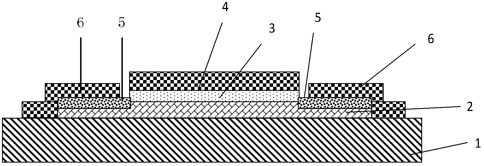
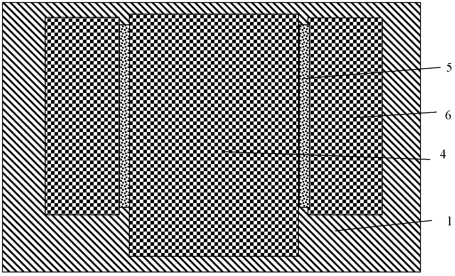
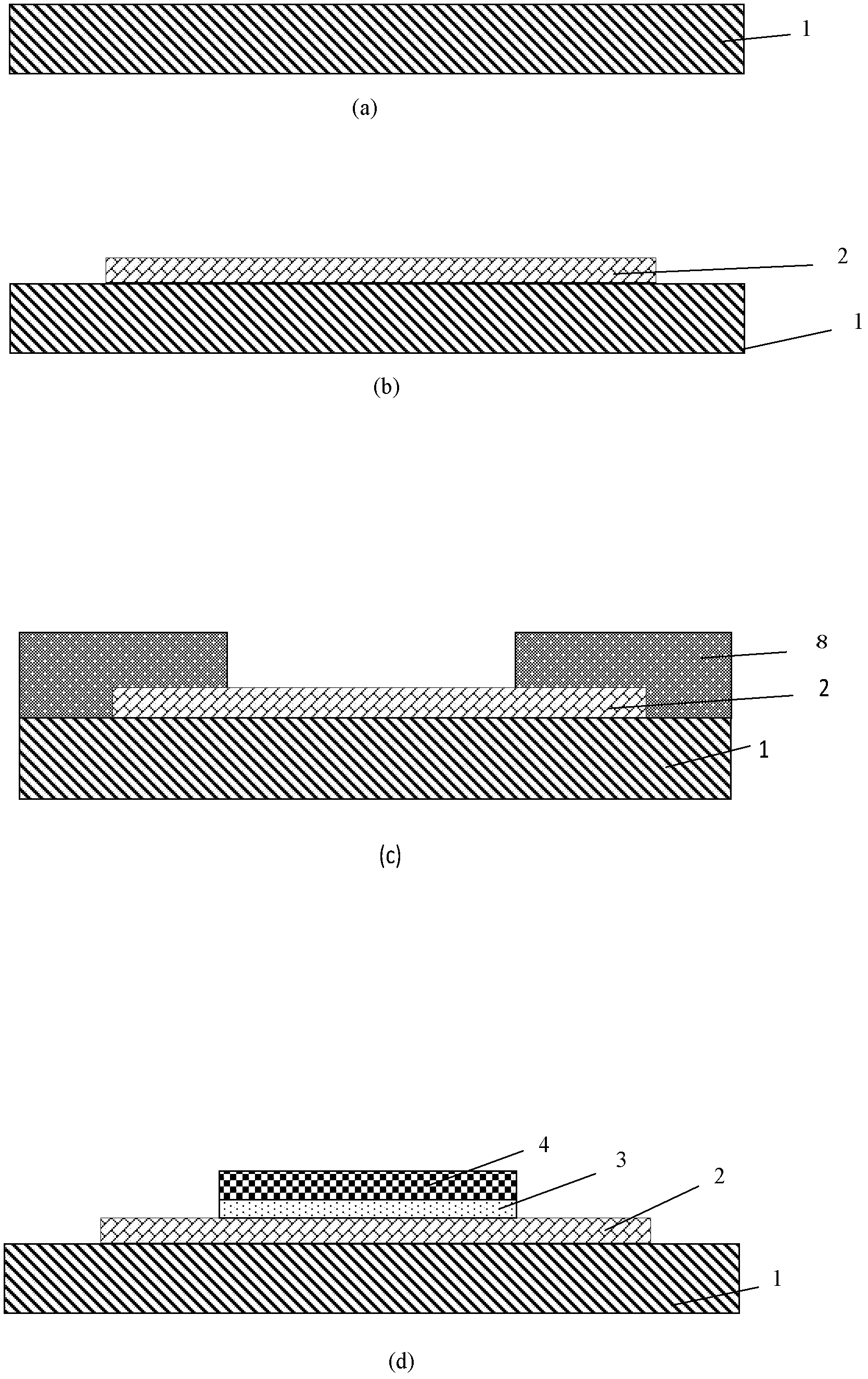
[0028] The self-aligned zinc oxide thin film transistor of the present invention is formed on the substrate 1 of glass, as figure 1 and figure 2 shown. The thin film transistor includes a semiconductor channel region 2 , a gate dielectric layer 3 , a gate electrode 4 , a source region and a drain region 5 with low resistance, and a source electrode and a drain electrode 6 . The semiconductor channel region 2 is located on the substrate 1, the gate dielectric layer 3 is located on the semiconductor channel region 2, the gate electrode 4 is located on the gate dielectric layer 3, the source electrode and the drain electrode 6 Located at both ends of the semiconductor channel region, the source and drain electrodes are naturally isolated from the gate electrode.

[0029] A specific example of the preparation method of the thin film tran...


PUM


Abstract

The invention discloses a preparation method for a top-gate self-aligned zinc oxide thin film transistor. According to the preparation method, only three masks are needed, and a zinc oxide thin film transistor is prepared through three times of photoetching; two layers of photoresist of a gate dielectric layer and a gate electrode outside a channel region are stripped together by adopting a self alignment process; and exposed semiconductor layers at two ends of the channel region are treated to reduce the resistance of the exposed semiconductor layers so as to form a low-resistance source region and a low-resistance drain region. Due to the implementation of self alignment of the gate dielectric layer and the gate electrode, parasitic capacitance and parasitic resistance are effectively reduced, and the grid-control capacity is improved; and therefore the preparation method has positive effects of improving the performance of a thin film transistor device, realizing a high-speed thin film transistor circuit and the like. Simultaneously, the process difficulty is greatly reduced, the manufacturing cost is saved, and the rate of finished products is improved.

Description

technical field [0001] The invention belongs to the fields of semiconductor industry and flat panel display, and in particular relates to a method for preparing a top gate self-aligned zinc oxide thin film transistor. Background technique [0002] Organic Light-Emitting Diode OLED (Organic Light-Emitting Diode) has self-illumination at the same time, no backlight is required, high contrast, thin thickness, wide viewing angle, fast response speed, can be used for flexible panels, wide operating temperature range, structure and process Simpler and other excellent features are considered to be the new application technology of the next generation of flat panel displays. However, it is impossible to meet these requirements if traditional amorphous silicon or polysilicon thin-film transistors or organic thin-film transistors are still used to drive OLEDs. For OLED display technology, many new technical requirements are put forward for thin film transistors: first, OLED devices r...

Claims


Application Information

Patent Timeline
Patent Type & Authority Applications(China)
IPC IPC(8): H01L21/336H01L21/28
Inventor 王漪蔡剑王薇韩德栋王亮亮任奕成张盛东刘晓彦康晋锋
Owner BOE TECH GRP CO LTD
Why Eureka
Try Eureka