High-reliability chip scale packaging method

A chip-level packaging and reliable technology, applied in the formation of wafer-level chip-scale packaging and the metal layer under solder bumps, can solve the problems of short-circuiting of solder bumps, easy dripping between solders, affecting soldering quality, etc. Adhesion, good wetting effect, effect of improving forming quality

Inactive Publication Date: 2012-05-02
NANTONG FUJITSU MICROELECTRONICS
View PDF3 Cites 13 Cited by
  • Summary
  • Abstract
  • Description
  • Claims
  • Application Information

AI Technical Summary

Problems solved by technology

[0012] In the process of forming wafer-level chip size packaging in the prior art, since the solder bump material is in direct contact with the metal wetting layer, the copper in the metal wetting layer easily diffuses into the tin of the solder bump to form a copper-tin alloy, which affects the welding quality
At the same time, before the solder is formed on the metal wetting layer, the exposed wetting layer is easily oxidized, which reduces the performance and reliability of the subsequently formed solder bumps
On the other hand, during the formation of solder bumps, the solder is easy to drip and affect the reliability of the product, especially for products with dense metal pads, the problem of short circuit between solder bumps is more likely to occur

Method used


Image

  • High-reliability chip scale packaging method
  • High-reliability chip scale packaging method
  • High-reliability chip scale packaging method

Examples


Embodiment Construction

[0029] The specific embodiments of the present invention will be described in detail below in conjunction with the accompanying drawings.

[0030] figure 2 It is a flow chart of a specific embodiment of the present invention to form solder bumps, including steps:

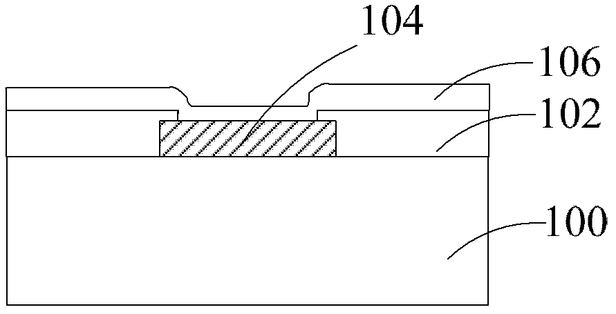
[0031] S101, sequentially forming a heat-resistant metal layer and a metal wetting layer on the chip pad and the passivation layer;

[0032] S102, forming a photoresist on the metal wetting layer, the photoresist is provided with an opening to expose the metal wetting layer above the chip pad;

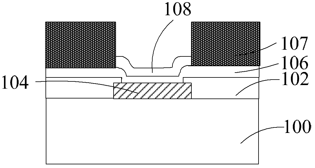
[0033] S103, sequentially forming a barrier layer and a solder protection layer on the metal wetting layer in the opening;

[0034] S104, removing the photoresist;

[0035] S105, etching the heat-resistant metal layer and the metal wetting layer on the passivation layer until the passivation layer is exposed;

[0036] S106, forming a protective glue layer on the chip, the protective glue covering the solder protective l...


PUM

PropertyMeasurementUnit
thicknessaaaaaaaaaa
thicknessaaaaaaaaaa

Abstract

The invention discloses a high-reliability chip scale packaging method. The method comprises the following steps: forming a heat-resisting metal layer and a metal wetting layer sequentially on a welding pad and a passivation layer on a chip; forming a photoresist on the metal wetting layer, wherein the photoresist is provided with the metal wetting layer with an opening exposed above the welding pad of the chip; forming a blocking layer and a welding flux protection layer sequentially on the metal wetting layer in the opening; removing the photoresist; etching the heat-resisting metal layer and the metal wetting layer which are positioned on the passivation layer until the passivation layer is uncovered; forming a protection adhesive layer on the chip, wherein the welding flux protection layer is covered by a protection adhesive; exposing the protection adhesive above a connection layer so as to form an opening, and uncovering the upper surface of the welding flux protection layer; and forming a welding flux bump on the welding flux protection layer and reflowing. According to the invention, the electric property and reliability of products are improved.

Description

technical field [0001] The invention relates to the field of semiconductor device packaging, in particular to a metal layer under a solder bump and a method for forming a wafer level chip scale package (Wafer Level chip Scale Package, WLCSP). Background technique [0002] In recent years, since the microcircuit manufacturing of chips is developing toward high integration, the chip packaging also needs to develop in the direction of high power, high density, thinness and miniaturization. Chip packaging means that after the chip is manufactured, the chip is wrapped in plastic or ceramic materials to protect the chip from external moisture and mechanical damage. The main functions of the chip package are power distribution, signal distribution, heat dissipation and protection support. [0003] Since today's electronic products are required to be light, thin, small and highly integrated, the fabrication of integrated circuits will be miniaturized, resulting in an increase in th...

Claims


Application Information

Patent Timeline
Patent Type & Authority Applications(China)
IPC IPC(8): H01L21/60H01L21/56
CPCH01L24/11H01L2224/11H01L2924/14H01L2924/00H01L2924/00012
Inventor 陶玉娟石磊高国华
Owner NANTONG FUJITSU MICROELECTRONICS
Why Eureka
Try Eureka