Method for forming solder bump

A solder bump and solder technology, which is applied in the field of semiconductor device packaging, can solve the problems affecting soldering quality, solder bump performance and reliability, and achieve the effects of improving forming quality, improving adhesion and good humidification.

Inactive Publication Date: 2012-06-13
NANTONG FUJITSU MICROELECTRONICS
View PDF5 Cites 0 Cited by
  • Summary
  • Abstract
  • Description
  • Claims
  • Application Information

AI Technical Summary

Problems solved by technology

[0006] In the process of forming wafer-level chip size packaging in the prior art, since the solder bump material is directly in contact with the metal wetting layer, the copper in the metal wetting layer easily diffuses into the tin of the solder bump to

Method used


Image

  • Method for forming solder bump
  • Method for forming solder bump
  • Method for forming solder bump

Examples


Embodiment Construction

[0023] The specific embodiments of the present invention will be described in detail below in conjunction with the accompanying drawings.

[0024] figure 2 It is a flow chart of a specific embodiment of the present invention to form solder bumps, including steps:

[0025] S101, sequentially forming a heat-resistant metal layer and a metal wetting layer on the chip pad and the passivation layer;

[0026] S102, forming a photoresist on the metal wetting layer, the photoresist is provided with an opening to expose the metal wetting layer above the chip pad;

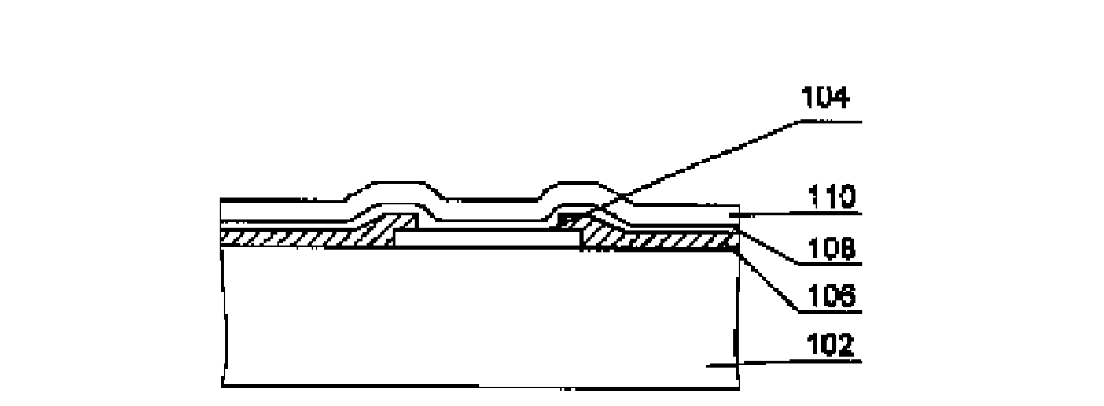
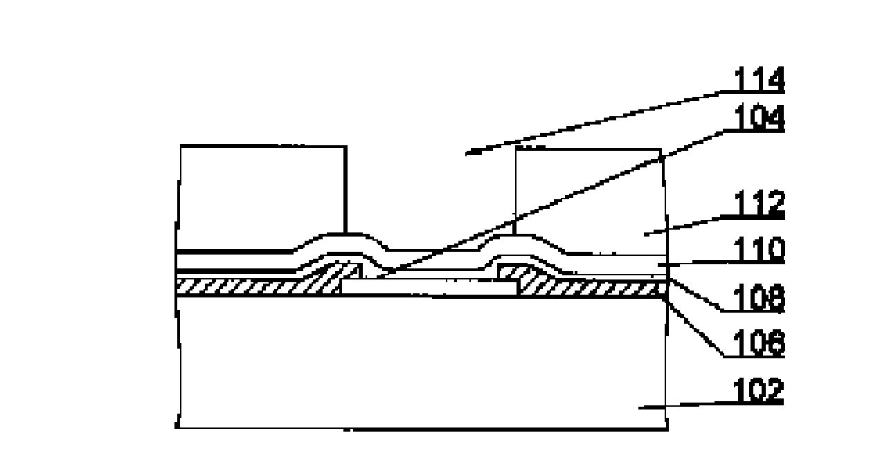
[0027] S103, sequentially forming a barrier layer and a solder protection layer on the metal wetting layer in the opening;

[0028] S104, forming a solder paste on the solder protection layer;

[0029] S105, removing the photoresist;

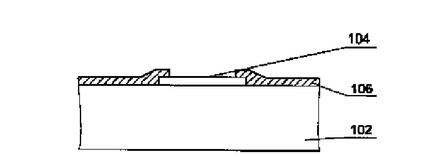
[0030] S106, etching the heat-resistant metal layer and the metal wetting layer on the passivation layer until the passivation layer is exposed;

[0031] S107 , reflowing the solder past...


PUM

PropertyMeasurementUnit
Thicknessaaaaaaaaaa
Thicknessaaaaaaaaaa

Abstract

The invention provides a method for forming a solder bump. The method comprises the following steps of: forming a heat resistant metal layer and a metal wetting layer on a pad and a passivation layer of a chip in sequence; forming a photoresist on the metal wetting layer, wherein the photoresist is provided with an opening to expose the metal wetting layer above the pad of the chip; forming a barrier layer and a solder protection layer on the metal wetting layer in the opening in sequence; forming solder paste on the solder protection layer; removing the photoresist; etching the heat resistant metal layer and the metal wetting layer on the passivation layer until the passivation layer is exposed; and ensuring the solder paste to reflow to form a solder bump. The method has the effect of improving the electrical property and reliability of the solder bump.

Description

technical field [0001] The invention relates to the field of semiconductor device packaging, in particular to a metal layer under a solder bump and a method for forming a wafer level chip scale package (Wafer Level chip Scale Package, WLCSP). Background technique [0002] In recent years, since the microcircuit manufacturing of chips is developing toward high integration, the chip packaging also needs to develop in the direction of high power, high density, thinness and miniaturization. Chip packaging means that after the chip is manufactured, the chip is wrapped in plastic or ceramic materials to protect the chip from external moisture and mechanical damage. The main functions of the chip package are power distribution, signal distribution, heat dissipation and protection support. [0003] Since today's electronic products are required to be light, thin, small and highly integrated, the fabrication of integrated circuits will be miniaturized, resulting in an increase in th...

Claims


Application Information

Patent Timeline
IPC IPC(8): H01L21/60
CPCH01L24/11H01L2224/11H01L2924/14H01L2924/00H01L2924/00012
Inventor 丁万春
Owner NANTONG FUJITSU MICROELECTRONICS
Why Eureka
Try Eureka