Low-power-consumption short pulse generation circuit and low-power-consumption pulse type D trigger

A technology for generating circuits and low power consumption. It is applied in the field of short pulse generating circuits. It can solve the problems of increasing power consumption of circuit transistors, increasing circuit power consumption, and increasing the number of circuit transistors, so as to reduce circuit power consumption, reduce the number of transistors, The effect of simple structure

Inactive Publication Date: 2012-05-02
NINGBO UNIV
View PDF4 Cites 15 Cited by
  • Summary
  • Abstract
  • Description
  • Claims
  • Application Information

AI Technical Summary

Problems solved by technology

Shinichi Kozu, Masayuki Daito, Yukinori Suglyama and others proposed a short pulse generation circuit with an AND gate structure. By making the clock signal and the complementary clock signal at the two input terminals of the AND gate be high at the same time in a short period of time, Thus, a short pulse signal is generated, and multiple inverters are cascaded at the output of the AND gate. Although a complementary clock signal with sufficient delay can be obtained, it also increases the number of circuit transistors and the power consumption of the circuit.
like figure 2 As shown, the short pulse generating circuit is composed of a PMOS transistor, an NMOS transistor, an AND gate and two inverters, wherein the AND gate is composed of a NAND gate and an inverter, and the The NAND gate is composed of two PMOS transistors and two NMOS transistors. The two PMOS transistors and the two NMOS transistors are all transistors with the minimum channel length under the standard process, but the NAND gate based on this structure has a short The pulse generation circuit needs to use multiple inverters to generate short pulse signals with sufficient pulse width. The increase of inverters leads to an increase in the number of transistors in the circuit, which leads to an increase in power consumption of the circuit

Method used


Image

  • Low-power-consumption short pulse generation circuit and low-power-consumption pulse type D trigger
  • Low-power-consumption short pulse generation circuit and low-power-consumption pulse type D trigger
  • Low-power-consumption short pulse generation circuit and low-power-consumption pulse type D trigger

Examples


Embodiment 1

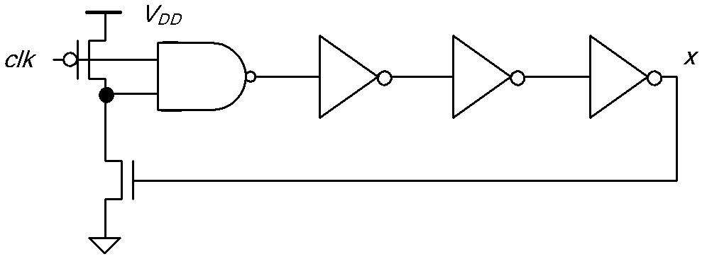
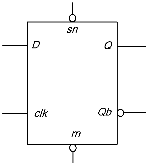
[0025] Embodiment one: if Figure 5 and Figure 6 As shown, a low-power short pulse generation circuit includes a first PMOS transistor P1, a first NMOS transistor N1, a first NAND gate U1 and a first inverter I1, the source of the first PMOS transistor P1 and the power supply Positive terminal V DD The first signal input terminal of the first NAND gate U1, the drain of the first PMOS transistor P1 and the drain of the first NMOS transistor N1 are connected, and the second signal input terminal of the first NAND gate U1 Connected to the gate of the first PMOS transistor P1, the source of the first NMOS transistor N1 is grounded, the signal output terminal of the first NAND gate U1, the signal input terminal of the first inverter I1 and the complementary pulse signal output terminal xb The three are connected, the signal output end of the first inverter I1, the gate of the first NMOS transistor N1 and the pulse signal output x are connected, the gate of the first PMOS transis...

Embodiment 2

[0026] Embodiment 2: other parts are the same as Embodiment 1, the difference is: the channel length of the second PMOS transistor P2, the channel length of the third PMOS transistor P3, the channel length of the second NMOS transistor N2 and the third The channel length of the NMOS transistor N3 is 1.3 times of the minimum channel length under the PTM90nm standard process.

Embodiment 3

[0027] Embodiment 3: other parts are the same as Embodiment 1, the difference is: the channel length of the second PMOS transistor P2, the channel length of the third PMOS transistor P3, the channel length of the second NMOS transistor N2 and the third The channel length of the NMOS transistor N3 is 1.4 times the minimum channel length under the PTM45nm standard process.

[0028] The working principle of the low power consumption short pulse generating circuit of the present invention is as follows:

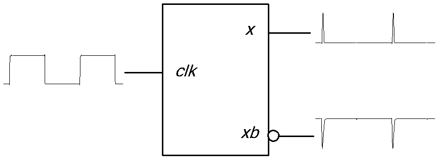
[0029] When the clock signal clk=0, the first PMOS transistor P1 is turned on, the drain of the first PMOS transistor P1 is charged to a high level, the first NAND gate U1 outputs the signal xb=1, and the first inverter I1 outputs the signal x= 0, the first NMOS transistor N1 is turned off.

[0030] When the clock signal clk=1, the first PMOS transistor P1 is closed, and the drain of the first PMOS transistor P1 is suspended. Since the drain of the first PMOS transistor P1 is ch...


PUM


Abstract

The invention discloses a low-power-consumption short pulse generation circuit and a low-power-consumption pulse type D trigger. The low-power-consumption short pulse generation circuit is characterized by comprising a first P-channel metal oxide semiconductor field effect transistor (PMOSFET), a first N-channel MOSFET (NMOSFET), a first NAND gate and a first phase inverter. The low-power-consumption pulse type D trigger is characterized by comprising the low-power-consumption short pulse generation circuit, an input phase inversion circuit, a clock control complementary MOS (CMOS) logic D latch unit and an output phase inversion circuit. The invention has the advantages that: under the condition of no influence of the performance of the circuit, the quantity of the transistors of the circuit is small; the structure is simpler; and the power consumption of the circuit is effectively reduced.

Description

technical field [0001] The invention relates to a short pulse generating circuit, in particular to a low power consumption short pulse generating circuit and a low power consumption pulse type D flip-flop. Background technique [0002] In recent decades, portable electronic devices have been widely used in the fields of consumer electronics, medical equipment and industrial instruments, and integrated circuits, as the core part of portable electronic devices, have developed rapidly. In the past integrated circuit design, the operating speed and area of ​​the chip are the main factors considered by the designer, and the power consumption problem is often ignored. With the continuous development of the semiconductor manufacturing industry, while the integration density and operating frequency of the circuit are gradually increasing, the dynamic power consumption and leakage power consumption of the chip are also increasing (see the literature Malay Ranjan Tripathy, "Nano CMOS"...

Claims


Application Information

Patent Timeline
Patent Type & Authority Applications(China)
IPC IPC(8): H03K3/012
Inventor 胡建平余晓颖邹凯裕
Owner NINGBO UNIV
Why Eureka
Try Eureka