Detection method and detection device for wafer level led chips and transparent probe card thereof

A technology for detecting light-emitting diodes and chips, which is applied in diode testing, measuring devices, measuring electricity, etc., can solve problems such as inability to improve efficiency, and achieve the effects of high sensitivity and optical rotation, simplified detection system, and improved rapid classification.

Active Publication Date: 2012-05-09
IND TECH RES INST
View PDF8 Cites 19 Cited by
  • Summary
  • Abstract
  • Description
  • Claims
  • Application Information

AI Technical Summary

Problems solved by technology

[0004] The technical problem to be solved by the present invention is to provide a wafer-level light-emitting diode chip detection method, detection device and its transparent probe card, which have the advantages of improving th

Method used


Image

  • Detection method and detection device for wafer level led chips and transparent probe card thereof
  • Detection method and detection device for wafer level led chips and transparent probe card thereof
  • Detection method and detection device for wafer level led chips and transparent probe card thereof

Examples


Embodiment Construction

[0043] Below in conjunction with accompanying drawing, structural principle and working principle of the present invention are specifically described:

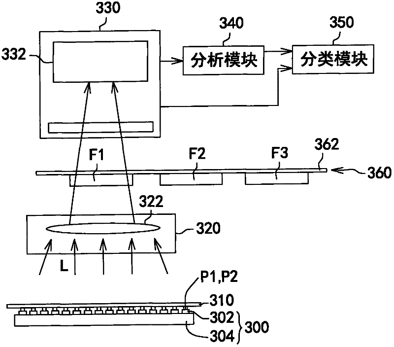
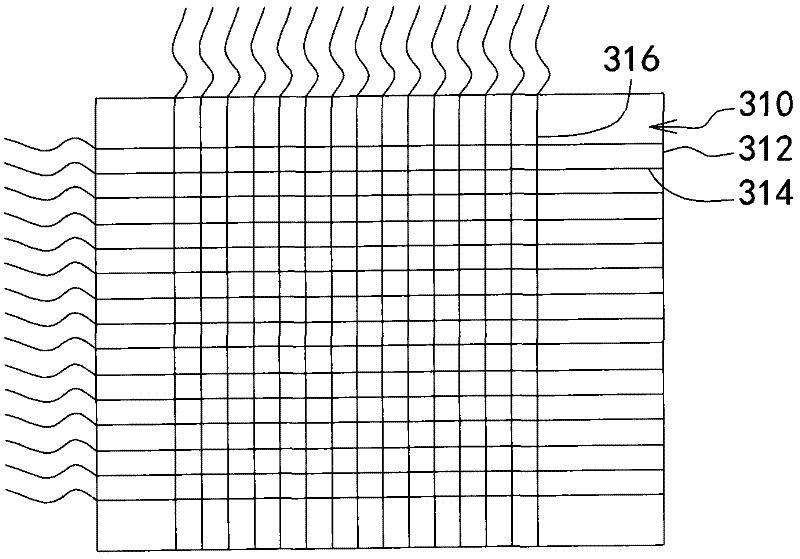
[0044] The wafer-level LED chip detection method, detection device and transparent probe card of the preferred embodiments of the present invention perform electrical analysis and lighting tests on the LED chips on the substrate. The detection method and device of the preferred embodiment of the present invention cited below uses a transparent probe card with an image processing module as the electrical detection unit and optical detection unit of the LED chip, and according to the obtained information of the spectrum and luminous intensity , to classify the plurality of LED chips.

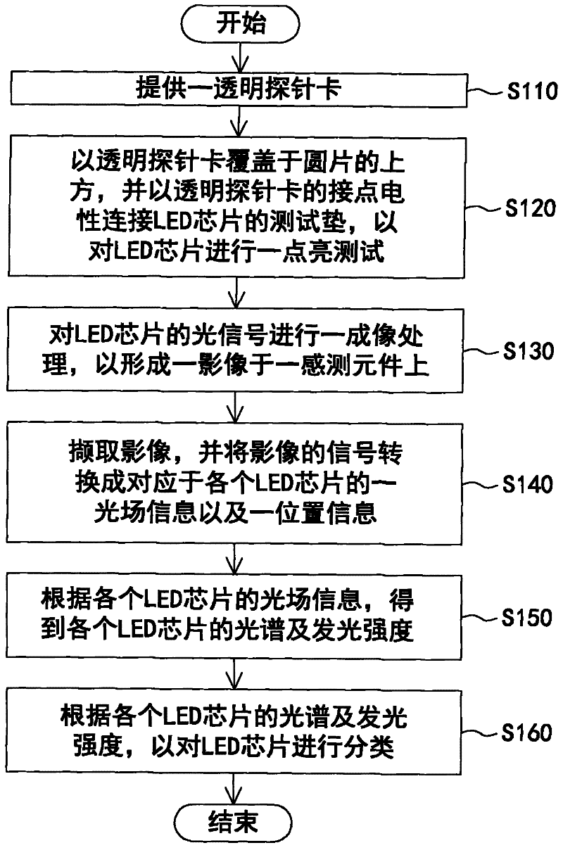
[0045] Please refer to figure 1 , which is a schematic flowchart illustrating a wafer-level LED chip inspection method according to a preferred embodiment of the present invention. The detection method includes the following steps S110-S160. Fi...


PUM


Abstract

The invention provides a detection method and a detection device for wafer level led chips and a transparent probe card thereof. A transparent probe card is provided and covers the wafer for electrically connecting the testing pads of the LED chips via the contacts so as to perform a light-up test on the LED chips. When the LED chips are lighted up, an imaging process is performed on the light signals of the LED chips to form an image on a sensing element. The image is captured, and the image signal is converted into an optical field information and a position information corresponding to each of the LED chips. The spectrums and the luminous intensities of the LED chips are obtained according to the optical field information of the LED chips. The LED chips are classified according to the spectrums and the luminous intensities of the LED chips. The invention also discloses a detection device for wafer level led chips applying the detection method and a transparent probe card. The detection method, the detection device, and the transparent probe card is provided with advantages of improved detection speed and quick classification.

Description

technical field [0001] The invention relates to a chip detection method, a detection device and a probe card thereof, and in particular to a wafer-level light emitting diode (Light emitting diode, LED) chip detection method, a detection device and a transparent probe card thereof. Background technique [0002] The existing LED chip detection method is to use a spot measuring device to spot-test the luminous characteristics of each LED chip on the wafer one by one. If there are about 2,000 LED chips in a 2-inch wafer, testing each LED chip one by one will take a long time and be inefficient. [0003] Existing point measuring devices, such as the point measuring structure disclosed in Chinese Taiwan Patent No. M382577 "Spot Measuring Device" and Chinese Taiwan Patent No. M260860 "Structure of Point Measuring System for Die After Cutting". The point measurement devices of the above patents are all for testing a single LED chip, and the system for testing the electrical and lum...

Claims


Application Information

Patent Timeline
IPC IPC(8): G01R31/44G01R1/073G01J1/42G01J3/28
CPCG01N21/9501G01N21/956G01R31/2635
Inventor 林建宪林宏彛彭耀祈郑佳申
Owner IND TECH RES INST
Why Eureka
Try Eureka