Bonding pad planarization process for improving packaging feasibility of bump structure
A flattening process and bonding pad technology, which is applied in the manufacturing of electrical components, electrical solid state devices, semiconductor/solid state devices, etc., can solve the problem that it is difficult to reduce bumps 16, etc., to increase feasibility and yield, and improve flatness Effect
- Summary
- Abstract
- Description
- Claims
- Application Information
AI Technical Summary
Problems solved by technology
Method used
Image

Examples
Embodiment Construction
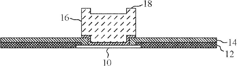
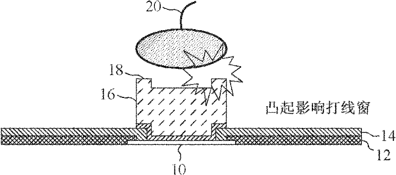
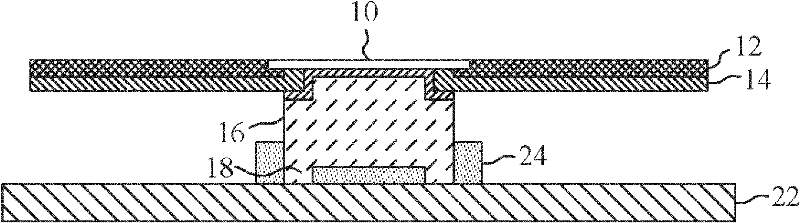
[0022] Figure 4A to Figure 4H It is a flowchart of the first embodiment of the present invention. After completing the front-end process of the wafer, such as Figure 4A As shown, the wafer passivation layer 12 and the rear passivation layer 14 cover the wafer, exposing only the bonding pads 10, which are usually aluminum. When making a bond pad, such as Figure 4B As shown, the barrier layer 262 and the seed layer 264 are sequentially sputtered. The barrier layer 262 can be titanium (Ti), titanium tungsten (TiW) or chromium (Cr), with a thickness between The seed layer 264 can be copper (Cu) or gold (Au), with a thickness between So far it is the same as conventional technology. Then a thick metal layer 30 of copper or gold is electroplated on the seed layer 264 to become Figure 4C structure shown. Preferably, the thickness of the thick metal layer 30 is greater than 3 μm. Then chemical mechanical polishing (CMP) the surface of the thick metal layer 30 becomes Fi...
PUM
| Property | Measurement | Unit |
|---|---|---|
| Thickness | aaaaa | aaaaa |
Abstract
Description
Claims
Application Information
 - Generate Ideas
- Intellectual Property
- Life Sciences
- Materials
- Tech Scout
- Unparalleled Data Quality
- Higher Quality Content
- 60% Fewer Hallucinations
Browse by: Latest US Patents, China's latest patents, Technical Efficacy Thesaurus, Application Domain, Technology Topic, Popular Technical Reports.
© 2025 PatSnap. All rights reserved.Legal|Privacy policy|Modern Slavery Act Transparency Statement|Sitemap|About US| Contact US: help@patsnap.com