Method for germanium-silicon epitaxy of high germanium concentration

A germanium-silicon epitaxy and germanium concentration technology, applied in chemical instruments and methods, from chemically reactive gases, single crystal growth, etc., can solve the problems of reduced production capacity, limited and high concentration of germanium, and achieve the effect of stable pressure control

Active Publication Date: 2012-05-23
SHANGHAI HUAHONG GRACE SEMICON MFG CORP
View PDF8 Cites 8 Cited by
  • Summary
  • Abstract
  • Description
  • Claims
  • Application Information

AI Technical Summary

Problems solved by technology

This may be based on the limitations of the following aspects. First, considering the high concentration of germanium on silicon germanium epitaxy, the mismatch is large, and it is easy to relax and generate defects; second, the reduction of the epitaxy temperature can increase the germanium concentration. Concentration, but the epitaxial growth rate will decrease a lot. We know from experiments that if the temperature is lowered by 30°C, the growth rate will be reduced to 1 / 3 of the original, which will reduce the production capacity. The concentration of germanium increases by 2% at ℃; thirdly, the concentration of germanium can be increased by increasing the flow rate of germane, but with the increase of flow rate of germane, the epitaxial growth rate increases, which makes the increase of germanium concentration limited. to the maximum, the germanium concentration increased by only 2%
Therefore, in the third method, if you want to achieve high germanium concentration, you must add a germane flowmeter. At present, we do 10% to 20% germanium concentration, because it is necessary to make a Ge gradient (that is, the germanium concentration gradually changes from high concentration to Low concentration), two germane flowmeters are already needed, so to do high germanium concentration epitaxy, at least three germane must be needed, which increases the equipment cost and process complexity

Method used


Image

  • Method for germanium-silicon epitaxy of high germanium concentration
  • Method for germanium-silicon epitaxy of high germanium concentration
  • Method for germanium-silicon epitaxy of high germanium concentration

Examples


Embodiment Construction

[0021] The present invention will be described in further detail below in conjunction with the accompanying drawings and embodiments.

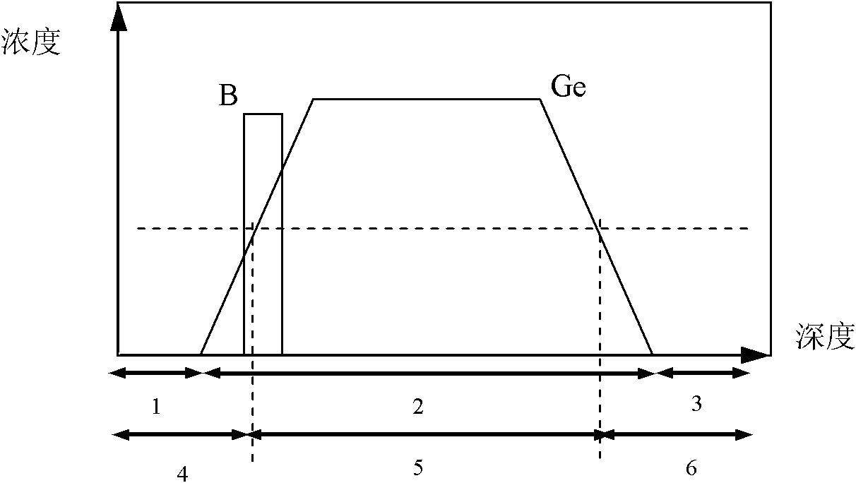
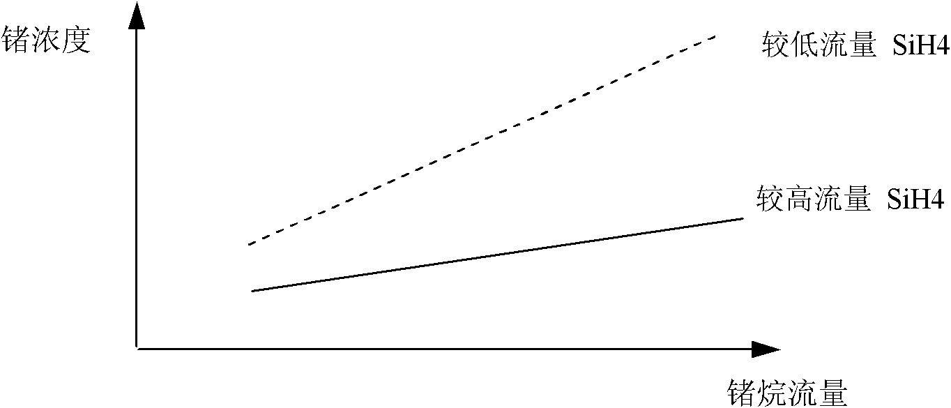
[0022] The invention discloses a silicon-germanium epitaxy method with high germanium concentration. When silane and germane gases are fed, the content of germanium (Ge) in the silicon-germanium epitaxy can be increased if the percentage of silane and germane is reduced. Such as figure 2 The schematic diagram of germanium doping concentration of different silicon source / germanium source ratios of the present invention is shown, at the same germanium source flow rate, as the silicon source flow rate decreases ( figure 2 Medium and low flow SiH 4 ), the concentration of germanium has a relatively large increase; at the same time, the concentration of germanium also increases with the increase of germanium flow rate, but the increase of germane flow rate has less influence on the increase of germanium concentration than the decrease of silane ...


PUM


Abstract

The invention discloses a method for a germanium-silicon epitaxy of high germanium concentration. According to the method, when silane and germane gases are introduced, the germanium content of a germanium-silicon epitaxy can be increased by lowering the percentages of silane and germane. At a same germanium source flow rate, and with the reduction of a silicon source flow rate, the germanium concentration is substantially enhanced, and finally a defect-free germanium-silicon epitaxial film with 25-35% of germanium atoms can be obtained. Under the premise of utilizing existing equipment, the method of the invention balances a growth rate and the doping concentration of germanium. While obtaining a high germanium concentration, the epitaxy growth rate is reduced by only a small degree. And the germanium-silicon epitaxy can be guaranteed to have no defect, meet device requirements, and have enough throughput simultaneously.

Description

technical field [0001] The invention belongs to a semiconductor manufacturing method, in particular to a silicon germanium epitaxy method with high germanium concentration. Background technique [0002] SiGe is another important semiconductor material after Si and GaAs. It has better characteristics than pure Si materials. The process and process can be compatible with silicon technology. The electrical performance of SiGe heterojunction bipolar transistor (HBT) is almost as good as It has reached the level of GaAs and other compound semiconductors to make similar devices. It has broad application prospects in the field of RF (radio frequency), especially ultra-high frequency, and it can be integrated with CMOS technology to give full play to the advantages of high integration and low cost of CMOS technology. At the same time It also achieves the high frequency performance and low noise performance of SiGe / Si HBTs. [0003] Because germanium has a narrow band gap (about 0.6...

Claims


Application Information

Patent Timeline
Patent Type & Authority Applications(China)
IPC IPC(8): C30B25/14C30B25/16C30B29/52
CPCC30B29/52C30B25/02
Inventor 缪燕季伟
Owner SHANGHAI HUAHONG GRACE SEMICON MFG CORP
Why Eureka
Try Eureka