Manufacture method of mesh transparent electrode

A transparent electrode and manufacturing method technology, applied in the direction of circuits, electrical components, semiconductor devices, etc., can solve the problems of thin film materials that are easy to fall off and affect the electrical performance of LED chips, so as to improve light extraction efficiency, eliminate residual stress, and improve overall quality. Effect

Inactive Publication Date: 2012-05-23
HAIDIKE NANTONG OPTOELECTRONICS TECH CO LTD
View PDF4 Cites 4 Cited by
  • Summary
  • Abstract
  • Description
  • Claims
  • Application Information

AI Technical Summary

Problems solved by technology

Due to the existence of large residual stress inside the LED epitaxial wafer, the film materials deposited later in the process, such as the transparent electrode layer ITO and the LED protective layer SiO2, are easy to fall off, which affects the electrical performance, optical performance, and reliability of the LED chip.

Method used


Image

  • Manufacture method of mesh transparent electrode
  • Manufacture method of mesh transparent electrode

Examples


Embodiment Construction

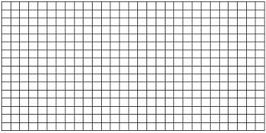
[0019] The manufacturing method of the mesh transparent electrode particularly includes the following steps: firstly, GaN material is deposited during the LED epitaxial growth process. Next, after the epitaxial growth of the LED is completed, a transparent electrode layer is deposited on the P-type region of the LED. The thickness of the transparent electrode layer is 300nm, the Ni mask is set on the outer surface of the transparent electrode layer by deposition method, the Ni mask is annealed to form a grid-like Ni mask, and the remaining Ni mask is used to cover the transparent electrode layer. The outer surface of the transparent electrode layer is etched, and then the deposited transparent electrode layer is made into a grid-like layer, that is, as figure 1 shown. Thus, the grid-like layer constitutes the current spreading layer and the stress buffering layer.

[0020] In this embodiment, a Ni mask is used to make the transparent electrode layer into a grid-like laye...


PUM

PropertyMeasurementUnit
thicknessaaaaaaaaaa
thicknessaaaaaaaaaa

Abstract

The invention relates to a manufacture method of a mesh-like transparent electrode, which is characterized by the following steps of: firstly, depositing a GaN material in an epitaxial growth process of an LED (Light-Emitting Diode); secondly, depositing a transparent electrode layer after the LED epitaxial growth; and finally, manufacturing the deposited transparent electrode layer to be a mesh-like layer. The mesh-like transparent electrode layer with a high dielectric constant is used as a current expansion layer and a stress buffering layer; therefore, the luminous efficiency is improved and the reliability of the device is further improved simultaneously. And more importantly, the invention can remove the larger residual stress existing inside an LED epitaxial wafer in the future, thereby preventing an LED protection layer from releasing and improving the entire quality of the LED.

Description

technical field [0001] The invention relates to a method for making an electrode, in particular to a method for making a mesh transparent electrode. Background technique [0002] In order to achieve the purpose of improving current transmission, it is necessary to make a current spreading layer under the LED electrodes in order to spread the current out of the electrodes. Usually, a transparent and conductive indium tin oxide film is used as the current spreading layer, and it is made on the upper surface of the chip by electron beam evaporation. At the same time, in order to protect the LED chip, a SiO2 film is usually deposited on the surface of the LED chip. [0003] In the process of LED epitaxial growth, due to the large lattice adaptation rate and large thermal expansion coefficient difference between the GaN material and the substrate sapphire, after the epitaxial wafer growth is completed, there is a large residual stress inside the LED epitaxial wafer . Due to th...

Claims


Application Information

Patent Timeline
Patent Type & Authority Applications(China)
IPC IPC(8): H01L33/00H01L33/38H01L33/40H01L33/42
Inventor 孙智江
Owner HAIDIKE NANTONG OPTOELECTRONICS TECH CO LTD
Why Eureka
Try Eureka