Multi-layer conductive transparent film and method for increasing light emitting efficiency of light emitting device

A technology of conductive transparent film and light extraction efficiency, applied in semiconductor devices, circuits, electrical components, etc., can solve problems such as affecting applications, poor P-type GaN ohmic contact, etc., to increase device size, reduce optical power loss, and improve light output. The effect of efficiency

Inactive Publication Date: 2012-05-30
HAIDIKE NANTONG OPTOELECTRONICS TECH CO LTD +1
View PDF5 Cites 1 Cited by
  • Summary
  • Abstract
  • Description
  • Claims
  • Application Information

AI Technical Summary

Problems solved by technology

However, the ohmic contact between P-type ZnO and P

Method used


Image

  • Multi-layer conductive transparent film and method for increasing light emitting efficiency of light emitting device
  • Multi-layer conductive transparent film and method for increasing light emitting efficiency of light emitting device
  • Multi-layer conductive transparent film and method for increasing light emitting efficiency of light emitting device

Examples


Embodiment Construction

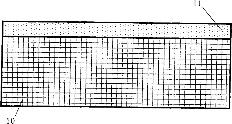
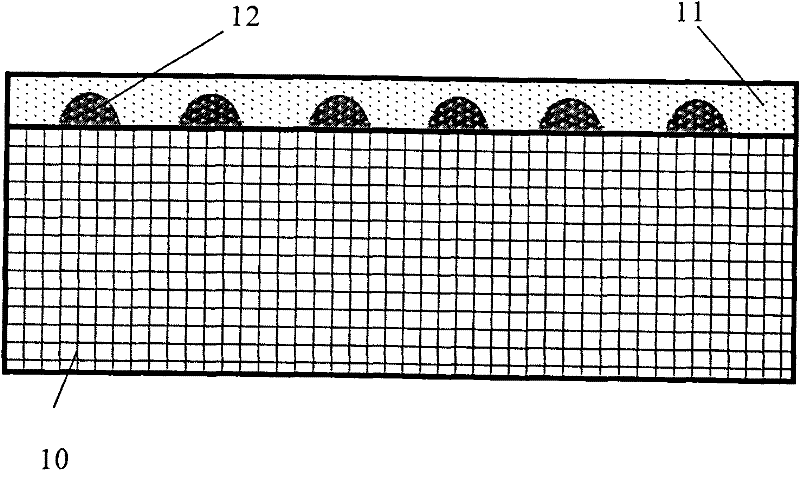
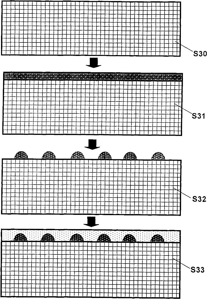
[0030] refer to figure 2 As shown, the multilayer conductive transparent film used to improve the light-emitting efficiency of the light-emitting device of the present invention also includes a high-refractive-index transparent electrode layer 12 grown on the P-type GaN surface epitaxial wafer 10, and then on the high-refractive-index transparent electrode layer 12 The outer surface of the ITO transparent electrode layer 11 is covered.

[0031] The main inventive point of the present invention is that a transparent electrode layer 12 with a high refractive index n>2.0 is sandwiched and grown between the P-type GaN surface epitaxial wafer 10 and the ITO transparent electrode layer 11 of the traditional GaN-based optoelectronic device. This transparent electrode layer 12 can select P-type ZnO electrode layer thin film for use (as: ZrO2-Y2O3, In2O3-Sb2O3, AlSb, GaSb, InGaSb, InSb, AlAs, InSb, AgBr, TlBr, AgCl, TlCl, CoSi2, TiSi etc.), The thickness of the P-type ZnO electrode l...


PUM

PropertyMeasurementUnit
Thicknessaaaaaaaaaa
Thicknessaaaaaaaaaa

Abstract

The invention discloses a multi-layer conductive transparent film and a method for increasing the light emitting efficiency of light emitting devices. The method comprises the steps of: growing a transparent electrode layer with a high refraction coefficient and an indium tin oxide (ITO) transparent electrode layer from inside to outside in sequence on an epitaxial wafer on a P-type gallium nitride (GaN) surface, wherein the refraction coefficient n of the transparent electrode layer is more than 2.0; and growing the transparent electrode layer by chemical vapor deposition or physical vapor deposition, making each of monomer electrodes into a microsphere or cone shape, and forming all transparent electrodes with high refraction coefficients into periodically arranged arrays by a photolithography-etching method, a selective growth method, a sol-gel method or a self-assembly method. Therefore, the light emitting efficiency of photoelectric devices is increased without the reduction of the electric properties of the photoelectric devices.

Description

technical field [0001] The invention relates to the technical field of manufacturing electronic components, in particular to a multilayer conductive transparent film capable of improving the light-emitting efficiency of a light-emitting device and a method thereof. Background technique [0002] Although GaN-based optoelectronic devices (LED light-emitting devices) have made considerable progress in recent years, it is difficult to achieve low-resistance P-type GaN ohmic contacts. There are two reasons for hindering low-resistance P-GaN ohmic contacts: on the one hand, it is difficult to grow heavily doped P-GaN materials (P-type concentration > 10 18 cm -3 ); on the other hand, there is a lack of suitable contact metal materials, the work function of P-GaN material is very large (7.5eV), and the metal Pt with the largest work function is only 5.6eV. In addition, the conditions of the metallization process (including surface treatment, metal deposition and alloying treat...

Claims


Application Information

Patent Timeline
IPC IPC(8): H01L33/42H01L33/00
Inventor 孙智江刘经国
Owner HAIDIKE NANTONG OPTOELECTRONICS TECH CO LTD
Why Eureka
Try Eureka