Lintel type dual-guide rail dual-drive stepping scanning double silicon wafer stage exchanging device and method thereof

A technology of double silicon wafer stage and silicon wafer stage, which is applied in the direction of photolithographic process exposure device, transportation and packaging, semiconductor/solid-state device manufacturing, etc., can solve the problem that the overall dynamic performance is greatly affected, the dynamic performance of the system is affected, and the large reaction of the base station problems such as force, to achieve the effect of shortening the processing cycle of a single chip, facilitating the control characteristics, and increasing the driving force

Inactive Publication Date: 2012-06-13
HARBIN INST OF TECH
View PDF11 Cites 2 Cited by
  • Summary
  • Abstract
  • Description
  • Claims
  • Application Information

AI Technical Summary

Problems solved by technology

In the patent CN101201555, the conveyor belt and the docking slider are used to complete the stage changing process, the movement rhythm is small, and the operation and maintenance are simple. However, the conveyor belt mechanism and the docking slider are fixed on the abutment, so there will be a large force during the stage changing process On the abutment, it has a great influence on the overall dynamic performance
In the patent CN1485694, the table-changing operation is completed by the docking of the Y-direction linear motor and the linear guide rail. However, due to the excessive gap in the middle of the abutment, a bridging device is introduced, which increases the movement rhythm and increases the time for table-changing. At the same time, the X-direction linear motor magnetically The steel part is fixed on the abutment, and the movement of the moving parts will generate a large reaction force on the abutment when the platform is changed, which in turn affects the dynamic performance of the entire system
In the patent CN101770181, the docking of the replacement unit is used to complete the work of changing the platform, but the guide device is fixed on the abutment. During the movement of changing the platform, the moving parts will generate a large reaction force on the abutment, which in turn affects the dynamic performance of the entire system.
Therefore, the current dual-platform solution needs to be improved.

Method used


Image

  • Lintel type dual-guide rail dual-drive stepping scanning double silicon wafer stage exchanging device and method thereof
  • Lintel type dual-guide rail dual-drive stepping scanning double silicon wafer stage exchanging device and method thereof
  • Lintel type dual-guide rail dual-drive stepping scanning double silicon wafer stage exchanging device and method thereof

Examples


Embodiment approach 1

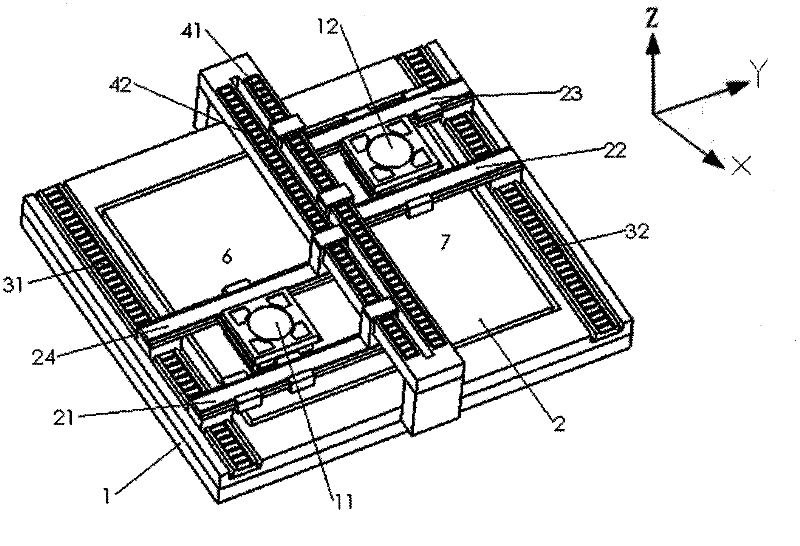
[0025] A lintel-type double-guided double-drive step-and-scan dual wafer stage exchange device, which includes a first wafer stage 11 running on the exposure station 6 and a first wafer stage 11 running on the pretreatment station 7 on the same base 1 The second silicon wafer stage 12 is characterized in that four first, second, third, and fourth linear motion units 21, 22, 23, and 24 in the Y direction are respectively arranged on the four edges of the base 1. The first and second linear motion units 31 and 32 in the X direction are respectively arranged on the two sides of the symmetry, and two lower bottom surfaces along the X direction are arranged on the middle part of the base 1 higher than the first and second silicon wafer stages 11. , the lintel-type first and second linear motion units 41, 42 of the 12 working surfaces; The linear motion units 21, 22, 23, 24 and the first and second linear motion units 31, 32 in the X direction perform X-Y motion in the plane enclose...

Embodiment approach 2

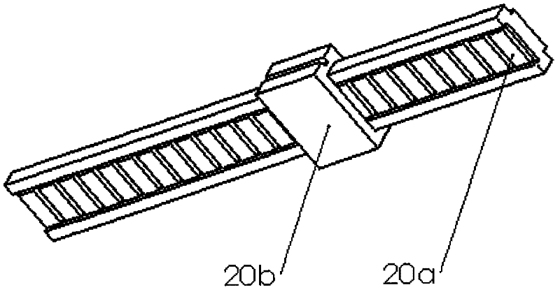
[0031] Such as Figure 10 As shown, the structure of the two beam-type X-direction linear motion units 41 and 42 placed in the middle of the abutment in Embodiment 1 is modified to obtain Embodiment 2. In Embodiment 1, the lintel-type X-direction linear motion units 41, 42 are composed of linear motors and air bearing guide rails, while in Embodiment 2, the new lintel-type X-direction linear motion units 41, 42 do not include linear motors structure, but only for air bearing rails. Compared with Embodiment 1, in Embodiment 2, the drive in the X direction is changed from double drive to single drive, because the double guide rail double drive mode is still adopted in the Y direction, so the advantages of large angular rigidity and torque resistance still exist; At the same time, because the single drive is used in the Y direction, the inconsistency of the driving force at both ends of the guide rail can be reduced to a certain extent; and, because the beam-type guide rail redu...


PUM


Abstract

The invention relates to a lintel type dual-guide rail dual-drive stepping scanning double silicon wafer stage exchanging device and a method thereof, and belongs to the field of semiconductor manufacturing equipment. According to the device, the system comprises two silicon wafer stages arranged on the same base station, wherein one silicon wafer stage operates at the exposure working position, and the other silicon wafer stage operates at the pretreatment working position; the edge of the base station is provided with 4 Y-direction linear movement units and 2 X-direction linear movement units; the middle of the base station is provided with 2 lintel type linear movement units, wherein the X directions of the lintel type linear movement units are higher than the working surfaces of the silicon wafer stages; the Y-direction linear movement units can perform the movements in the X direction through the X-direction linear movement units, and can collectively perform the movements of thesilicon wafer stages in the X direction or in the Y direction with Y-direction movement sliders of the Y-direction linear movement units. According to the present invention, the torsion interference resistance of the guide rail can be enhanced, the movement deviation and the deformation deviation can be decreased or overcome, and the movement precision of the silicon wafer stage can be improved; the operation of the device of the present invention only comprises three steps so as to shorten the required double stage exchanging time, and significantly improve the production efficiency of the photoetching machine.

Description

technical field [0001] The invention belongs to the technical field of semiconductor manufacturing equipment, and mainly relates to a lintel-type double-guide rail double-drive step-scanning double-silicon wafer stage exchanging device and method. Background technique [0002] Photolithography technology is to transfer the pattern on the mask plate to the photoresist coated on the surface of the silicon wafer by exposure method, and transfer the pattern on the photoresist to the silicon wafer by subsequent development, etching and other technologies. Lithography machine is one of the important ultra-precision system engineering equipment in lithography technology, and its overall performance plays a very important role in the whole lithography process. The main function of the silicon wafer stage is to carry the wafer under the condition of high speed and high acceleration to achieve nanoscale positioning, complete the processes of loading and unloading, pre-alignment, align...

Claims


Application Information

Patent Timeline
Patent Type & Authority Applications(China)
IPC IPC(8): G03F7/20H01L21/67H01L21/677
Inventor 谭久彬王绍凯崔继文
Owner HARBIN INST OF TECH
Why Eureka
Try Eureka