Wafer bearing structure and preparation method thereof, and wafer thinning method

A wafer carrying and wafer technology, which is applied in semiconductor/solid-state device manufacturing, electrical components, circuits, etc., can solve the problem that the wafer carrying structure cannot meet the requirements of TSV process, and reduce the requirements for surface flatness and reduce costs , The effect of saving process

Active Publication Date: 2015-01-14
FUDAN UNIV
View PDF4 Cites 0 Cited by
  • Summary
  • Abstract
  • Description
  • Claims
  • Application Information

AI Technical Summary

Problems solved by technology

[0019] The purpose of the present invention is to provide a wafer carrying structure and its preparation method and wafer thinning method to solve the problem that the existing wafer carrying structure cannot meet the requirements of the TSV process

Method used


Image

  • Wafer bearing structure and preparation method thereof, and wafer thinning method
  • Wafer bearing structure and preparation method thereof, and wafer thinning method
  • Wafer bearing structure and preparation method thereof, and wafer thinning method

Examples


Embodiment 1

[0070] Please refer to figure 2 and Figure 3A to Figure 3D ,in, figure 2 A flow chart of the method for preparing the wafer carrying structure provided in the first embodiment of the present invention, Figure 3A to Figure 3D The sectional view of the wafer carrying structure corresponding to each step of the method for preparing the wafer carrying structure provided in the first embodiment of the present invention, combined with figure 2 and Figure 3A to Figure 3D , the preparation method of the wafer carrying structure provided by the first embodiment of the present invention includes the following steps:

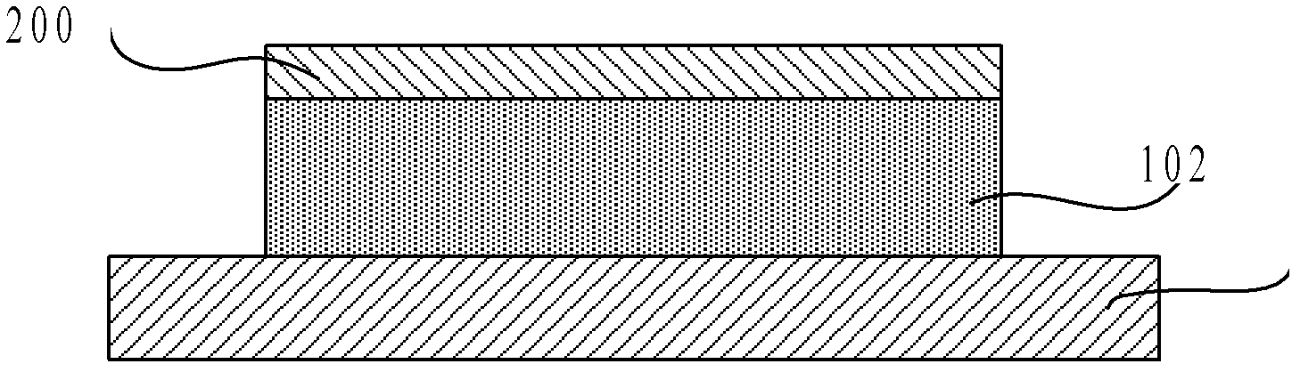
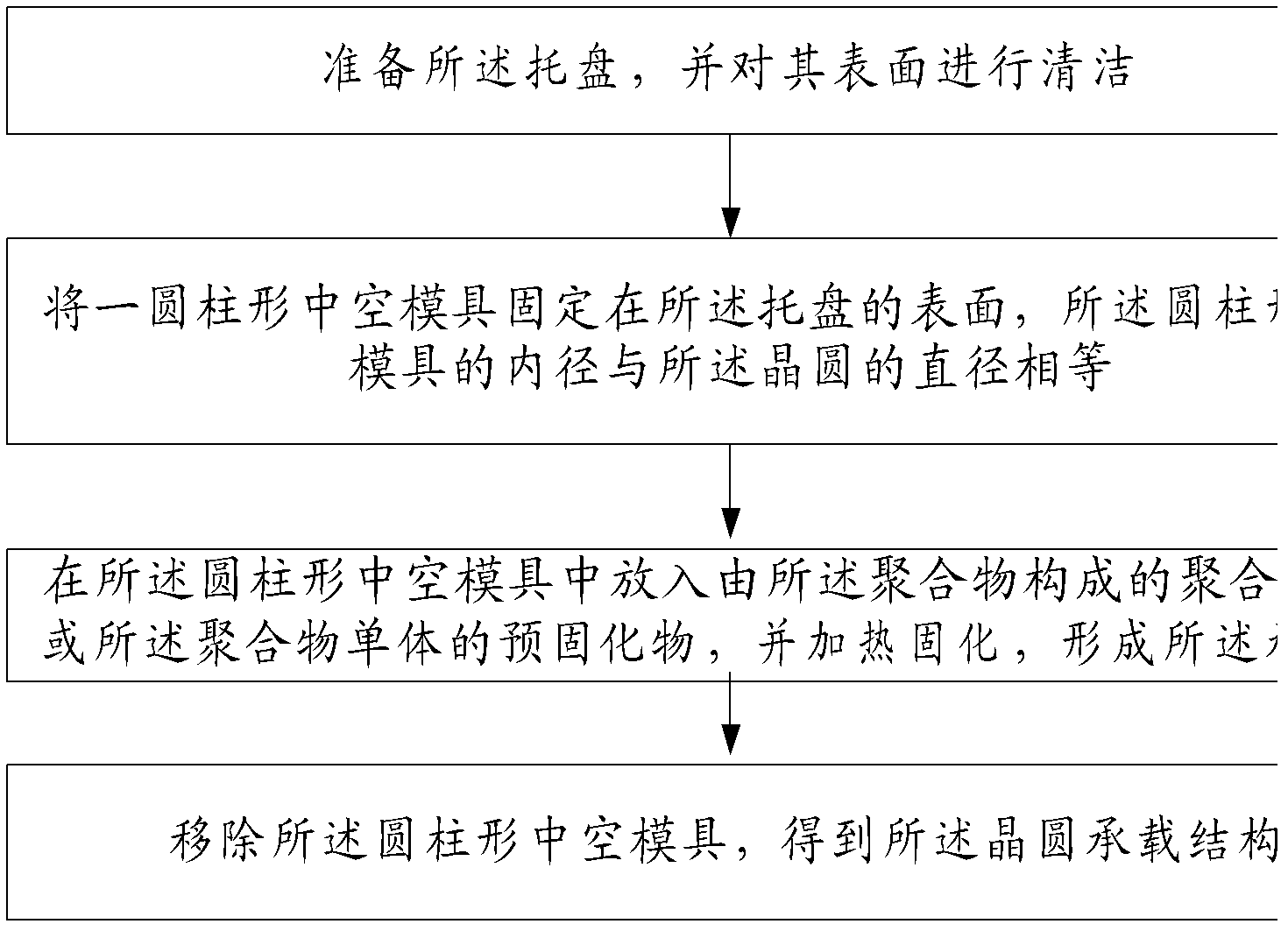
[0071] S101, prepare the tray 101, and clean its surface, such as Figure 3A shown;

[0072] S102. Fix a cylindrical hollow mold 300 on the surface of the tray 101, the inner diameter of the cylindrical hollow mold 300 is equal to the diameter of the wafer, as Figure 3B Shown; Wherein, the height of described cylindrical hollow mold is 10~15mm.

[0073] S103....

Embodiment 2

[0076] The difference between embodiment 2 and embodiment 1 is that: the carrier plate is prepared first, and then the carrier plate is fixed on the tray, specifically, the carrier plate can be adhered to the tray . That is, the preparation method of the wafer carrying structure provided in Example 2 comprises the following steps:

[0077] Prepare the pallet and clean its surface;

[0078] Prepare the carrier plate; specifically, first prepare a cylindrical hollow mold, the inner diameter of the cylindrical hollow mold is equal to the diameter of the wafer; The polymer monomer or the pre-cured product of the polymer monomer is heated and cured to form the carrier plate; wherein, the height of the cylindrical hollow mold is 10-15 mm;

[0079] The carrier plate is adhered to the tray to form the wafer carrier structure.

[0080] Please continue to refer Figure 4 and Figure 5A to Figure 5D ,in, Figure 4 The flow chart of the wafer thinning method provided by the embodime...


PUM


Abstract

The invention discloses a wafer bearing structure. The structure comprises: a pallet and a bearing tray fixed on the pallet. A wafer to be processed is fixed on the bearing tray. A requirement to surface smoothness of the pallet is reduced. The pallet is protected to not be damaged during a wafer processing process. Repeatable utilization can be achieved and cost can be saved. Simultaneously, the invention also discloses a preparation method of the wafer bearing structure. The method is characterized by: placing a polymer monomer or a precuring object of the polymer monomer in a cylindrical hollow moldm, heating and curing; directly forming the bearing tray on the pallet or fixing the bearing tray on the pallet through bonding after the bearing tray is formed. The method is simple and convenient. And the invention also provides a wafer thinning method. According to the wafer thinning method, the above wafer bearing structure is used to bear the wafer in the wafer processing technology. The wafer thinning method is convenient and reliable and is completely compatible with the current wafer thinning and through silicon via processing technology.

Description

technical field [0001] The invention relates to the technical field of semiconductor packaging, in particular to a wafer carrying structure, a preparation method thereof, and a wafer thinning method. Background technique [0002] With the improvement of the integration level of silicon chips, the size of semiconductor devices is getting smaller and smaller. When the characteristic line width of silicon integrated circuits enters the nanometer scale (such as below 50 nanometers), silicon microelectronics technology will be limited and challenged from physical aspects. . Therefore, it becomes very important to further realize the miniaturization and miniaturization of electronic systems through packaging technology. [0003] In the field of packaging technology, improving the integration of electronic systems through three-dimensional and system-in-package has become the development direction of miniaturization and multi-function of electronic products. Among them, the reali...

Claims


Application Information

Patent Timeline
Patent Type & Authority Patents(China)
IPC IPC(8): H01L21/683H01L21/304
Inventor 杨东伦肖斐
Owner FUDAN UNIV
Why Eureka
Try Eureka