
Dual dielectric tri-gate field effect transistor

A technology of field effect transistor and double dielectric, applied in the field of tri-gate field effect transistor, can solve the problem of current increase and other problems

Active Publication Date: 2012-06-13
GLOBALFOUNDRIES INC
View PDF7 Cites 4 Cited by
  • Summary
  • Abstract
  • Description
  • Claims
  • Application Information

AI Technical Summary

Problems solved by technology

Also, since the sidewalls act as gate regions, the potential increase in current available per plane layout

Method used


Image

  • Dual dielectric tri-gate field effect transistor
  • Dual dielectric tri-gate field effect transistor
  • Dual dielectric tri-gate field effect transistor

Examples


Embodiment Construction

[0020] In the following description, numerous specific details are set forth, such as particular structures, components, materials, dimensions, processing steps and techniques, in order to provide a thorough understanding of the present invention. However, it will be understood by those skilled in the art that the present invention may be practiced with a wide variety of specific details. In other instances, well-known structures or process steps have not been described in detail in order to avoid obscuring the invention.

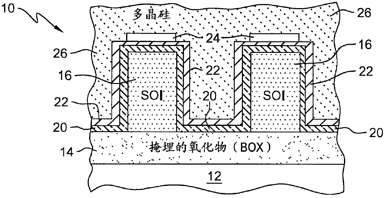
[0021] figure 1 A dual dielectric tri-gate structure according to one embodiment of the invention is shown. Structure 10 includes a base semiconductor substrate 12 , an insulator layer 14 , a plurality of semiconductor fins 16 , a high-k dielectric 20 , a metal layer 22 , a top gate dielectric 24 , and a gate electrode 26 .

[0022] The base semiconductor substrate layer 12 may comprise any semiconductor material, including but not limited to: Si, SiC, Si...


PUM


Abstract

A dual dielectric tri-gate field effect transistor, a method of fabricating a dual dielectric tri-gate field effect transistor, and a method of operating a dual dielectric tri-gate effect transistor are disclosed. In one embodiment, the dual dielectric tri-gate transistor comprises a substrate, an insulating layer on the substrate, and at least one semiconductor fin. A first dielectric having a first dielectric constant extends over sidewalls of the fin, and a metal layer extends over the first dielectric, and a second dielectric having a second dielectric constant is on a top surface of the fin. A gate electrode extends over the fin and the first and second dielectrics. The gate electrode and the first dielectric layer form first and second gates having a threshold voltage Vt1, and the gate electrode and the second dielectric layer form a third gate having a threshold voltage Vt2 different than Vt1.

Description

technical field [0001] The present invention relates generally to semiconductor devices, and more particularly to tri-gate field effect transistors. Background technique [0002] Due to the increasing difficulty in controlling leakage current while shrinking the gate length of complementary metal-oxide-semiconductor (CMOS) transistors, traditional single-gate metal-oxide-semiconductor field-effect transistor (MOSFET) structures can be replaced with double- or triple-gate MOSFET structure instead. These structures allow greater ability to turn off MOSFETs with ultra-short channel lengths by increasing gate control of the channel potential. Among the various multi-gate MOSFET structures developed in recent years, the most promising in terms of manufacturability and performance is the variation of the so-called "FinFET" structure. In these devices, a strip or "fin" of silicon is formed, and the gate material is subsequently deposited and etched such that the resulting gate su...

Claims


Application Information

Patent Timeline
Patent Type & Authority Applications(China)
IPC IPC(8): H01L29/78H01L21/336H01L21/84H01L27/12
CPCH01L29/785H01L29/66795H01L21/84H01L27/1203H01L2924/0002H01L2924/00
Inventor J·斯莱特J·常L·常C-H·林
Owner GLOBALFOUNDRIES INC
Learn More