
Method for measuring dark signal non-uniformity and photon response non-uniformity of photons of CCD (charge coupled device) chip

A non-uniformity and dark signal technology, applied in the field of measurement, can solve problems containing spectrally related information, differences, and inextricability

Inactive Publication Date: 2012-06-20
XIDIAN UNIV
View PDF2 Cites 21 Cited by
  • Summary
  • Abstract
  • Description
  • Claims
  • Application Information

AI Technical Summary

Problems solved by technology

[0003] The traditional measurement of CCD chip dark signal non-uniformity and photon response non-uniformity parameters all use a wide-spectrum light source as the light source, which cannot exclude the influence of spectral-related factors in the final measurement parameters, resulting in spectral-related information in the measured parameters , and the current measurement method generally places the CCD chip in a normal temperature environment for measurement, without considering the ambient temperature of the CCD chip, resulting in a certain difference between the measured parameters and the actual parameters when the CCD chip is in a specific working environment

Method used


Image

  • Method for measuring dark signal non-uniformity and photon response non-uniformity of photons of CCD (charge coupled device) chip
  • Method for measuring dark signal non-uniformity and photon response non-uniformity of photons of CCD (charge coupled device) chip
  • Method for measuring dark signal non-uniformity and photon response non-uniformity of photons of CCD (charge coupled device) chip

Examples


Embodiment Construction

[0038] CCD chip is a widely used imaging device, which is widely used in many fields such as astronomy, aerospace, biological and medical research, molecular dynamics, spectroscopy, underwater photography, X-ray detection, etc. For this reason, the performance parameters of CCD chip It is critical to conduct an assessment. At present, the evaluation of CCD chips mainly includes the following parameters:

[0039] ①Quantum efficiency η: The ratio of the number of photoelectrons generated by the CCD under the irradiation of wavelength λ to the number of incident photons. This parameter characterizes the response ability of the CCD chip to monochromatic light of a specific wavelength.

[0040] ②Responsivity parameter R: The ratio of the signal voltage to the exposure amount of the CCD under the illumination of monochromatic light of a given wavelength. This parameter generally describes the CCD quantum efficiency and system gain.

[0041] ③Saturation μ p.sat : The number of pho...


PUM


Abstract

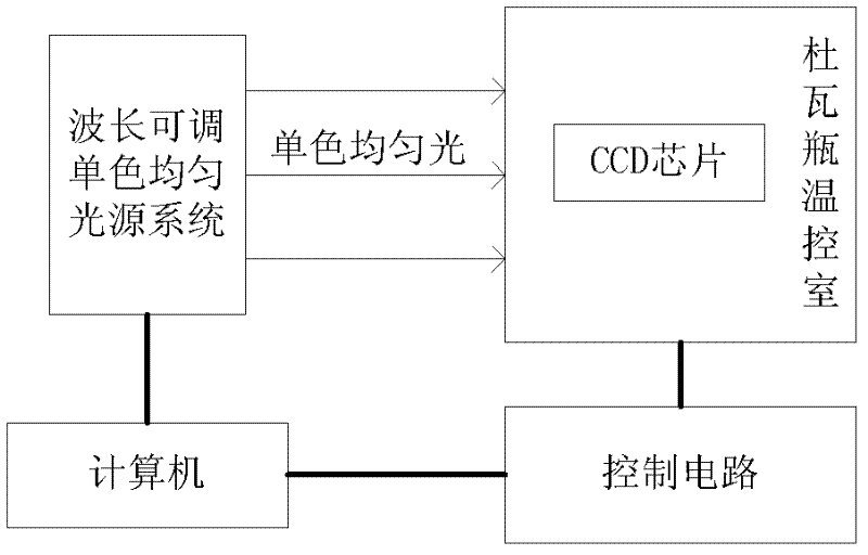
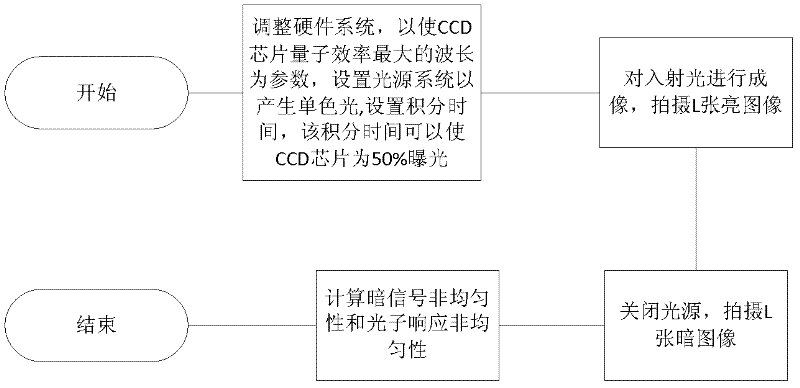
The invention discloses a method for measuring dark signal non-uniformity and photon response non-uniformity of a CCD (charge coupled device) chip, which mainly solves the problem of insufficient measurement precision of performance parameters of a CCD of the prior art. The method includes steps of selecting the wavelength eta corresponding to the maximum quantum efficiency of the CCD chip, setting a wavelength-adjustable monochromatic uniform light source, and generating monochromatic light with the wavelength eta; then selecting integration time required to realize 50% exposure of the CCD chip, and adopting the integration time as a parameter to control the CCD chip to shoot two groups of image sequences and upload the two groups of image sequences to a computer; and computing parameters of the dark signal non-uniformity DSNU and the photon response non-uniformity PRNU of the CCD chip by means of computing a total average gray value and a spatial variance according to the two groups of images. The method has the advantages of high measurement precision and fine stability, and can be used for assessing performances of CCD chips.

Description

technical field [0001] The invention belongs to the field of measurement technology, in particular to the measurement of CCD chip dark signal non-uniformity DSNU and photon response non-uniformity PRNU parameters, which is used for the development, evaluation and screening of CCD chips. Background technique [0002] In the development and application of CCD chips, due to the limitations of processing and measurement technology, the actual quantum efficiency and responsivity parameters of CCD chips are different from the measured values ​​given by the manufacturer. In some key application fields, quantitative understanding is required. The actual performance parameters of the CCD chip, so as to make reasonable corrections to the collected data and obtain better and more accurate data. Therefore, it is necessary to propose a method to effectively measure the dark signal non-uniformity and photon response non-uniformity parameters of the CCD chip. Through these two performance ...

Claims


Application Information

Patent Timeline
Patent Type & Authority Applications(China)
IPC IPC(8): G01R31/26G01M11/02
Inventor 邵晓鹏王阳张临临王杨杨晓晖范华卢光旭马菁汀吕斐许宏涛
Owner XIDIAN UNIV
Learn More