Cellular electric fusion chip device based on dispersed type side wall microelectrode array and processing process

A technology of microelectrode array and electrofusion, applied in stress-stimulated microbial growth methods, biochemical equipment and methods, biochemical instruments, etc., to achieve good flow characteristics, realize efficient queuing control and efficient fusion, and ensure reliability

Inactive Publication Date: 2012-06-27
CHONGQING UNIV
View PDF8 Cites 1 Cited by
  • Summary
  • Abstract
  • Description
  • Claims
  • Application Information

AI Technical Summary

Problems solved by technology

[0012] The purpose of the present invention is to address the deficiencies of the prior art, and propose a cell electrofusion chip device and its processing technology based on a discrete sidewall microelectrode array. Silicon and filled polysilicon form an insulating isolation structure, and a discrete sidewall microelectrode array is formed by dry etching. The discrete sidewall microelectrode array and the insulating isolation structure together form the sidewall of the microchannel, which not only ensures The array forms a non-uniform electric field inside the microchannel, and forms a smooth linear microchannel side wall, avoiding the cell blockage problem caused by the traditional toothed microelectrode structure

Method used


Image

  • Cellular electric fusion chip device based on dispersed type side wall microelectrode array and processing process
  • Cellular electric fusion chip device based on dispersed type side wall microelectrode array and processing process
  • Cellular electric fusion chip device based on dispersed type side wall microelectrode array and processing process

Examples


Embodiment Construction

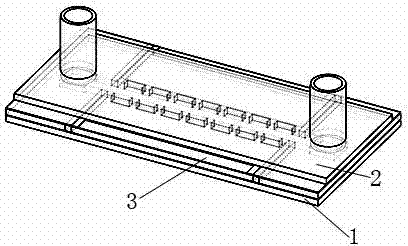
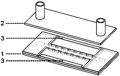
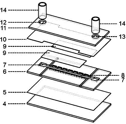
[0044] see Figure 1 to Figure 4 , the cell electrofusion chip device based on the discrete sidewall microelectrode array is composed of the cell electrofusion chip 1 and the flow path control layer 2 based on the discrete sidewall microelectrode array.

[0045] Cell electrofusion chip 1 based on discrete sidewall microelectrode arrays has a silicon base layer 4, a silicon dioxide insulating layer 5, and a top low-resistance silicon layer 6 from bottom to top (including discrete sidewall microelectrode arrays, insulation isolation structure and microchannel), aluminum lead layer 9, silicon dioxide passivation layer 10.

[0046] The silicon base layer 4 is selected to have a diameter of 3 to 4 For SOI wafers, the function of the silicon base layer is to provide a mechanical support layer with a thickness of 300-450 μm.

[0047] The silicon dioxide insulating layer 5 has a thickness of 0.5-2 μm, and its function is to provide good electrical insulation performance.

[0048] ...


PUM

PropertyMeasurementUnit
thicknessaaaaaaaaaa
thicknessaaaaaaaaaa
thicknessaaaaaaaaaa

Abstract

A cellular electric fusion chip device based on a dispersed type side wall microelectrode array is composed of a cellular electric fusion chip and a flow path control layer. The cellular electric fusion chip is provided with a silicon substrate layer, a silicon dioxide insulating layer is arranged on the silicon substrate layer, a top layer low-resistivity silicon layer is positioned on the silicon dioxide insulating layer, a microchannel is disposed in the top layer low-resistivity silicon layer and enables the silicon dioxide insulating layer to serve as the bottom, and toothed side wall microelectrodes are oppositely arranged on two sides of the microchannel. Insulating isolation structures are adopted between the adjacent toothed side wall microelectrodes to separate low-resistivity silicon from the toothed side wall microelectrodes, the end face of the separated low-resistivity silicon is flush with the end faces of the toothed side wall microelectrodes so that the microchannel is a smooth channel. The chip guarantees that the toothed side wall microelectrodes array forms an un-uniform electric field in the microchannel, a smooth linear microchannel side wall is formed, and the problem of cell blockage caused by a traditional toothed microelectrode structure can be solved.

Description

technical field [0001] The invention relates to a cell electrofusion chip device based on a discrete sidewall microelectrode array and its processing technology. Its main application scope is the fusion cell preparation of animal, plant, and microbial cells, and it can also be applied to electroporation, electroporation, etc. It can be widely used in genetics, animal and plant distant hybrid breeding, developmental biology, drug screening, monoclonal antibody preparation, mammalian cloning and other fields. Background technique [0002] Since the 1980s, cell electrofusion technology has been rapidly developed and widely used because of its advantages such as high efficiency, easy operation, non-toxic to cells, easy observation, suitable for instrument application and standardized operation (see 4326934, April 27, 1982, Pohl; 441972, April 10, 1982, Pohl; 4578168, March 25, 1986, Hofman; 4695547, Sep 22, 1987, Hillard; 4699881, Oct 13, 1987, Matschke, et al. ;). [0003] Ce...

Claims


Application Information

Patent Timeline
Patent Type & Authority Applications(China)
IPC IPC(8): C12M1/42
CPCC12M35/02
Inventor 胡宁徐静杨军郑小林侯文生廖彦剑杨静胡南
Owner CHONGQING UNIV
Why Eureka
Try Eureka