Data split method and correction method of stepping photoetching mask plate for diagrammed substrate process

A technology for patterning substrates and photolithography masks, which is applied in the photoengraving process of the pattern surface, the originals for opto-mechanical processing, optics, etc. Avoid edge effects, improve quality, good overall stitching effect

Active Publication Date: 2014-02-05
NO 55 INST CHINA ELECTRONIC SCI & TECHNOLOGYGROUP CO LTD
View PDF4 Cites 6 Cited by
  • Summary
  • Abstract
  • Description
  • Claims
  • Application Information

AI Technical Summary

Problems solved by technology

Due to the optical edge effect at the edge of the exposure window, there is a certain numerical error in the production and use of the photolithography mask. Therefore, on the semiconductor material after the splicing exposure, the splicing traces on the circle can be clearly seen, resulting in Decreased consistency of graphics across the material, reducing yield

Method used


Image

  • Data split method and correction method of stepping photoetching mask plate for diagrammed substrate process
  • Data split method and correction method of stepping photoetching mask plate for diagrammed substrate process
  • Data split method and correction method of stepping photoetching mask plate for diagrammed substrate process

Examples


specific Embodiment approach

[0021] Specific implementation methods (take the PSS plate with a 10-micron circle and a pitch of 5 microns as an example)

[0022] The first step is to determine the diameter (eg: 10 microns) and spacing size (eg: 5 microns) of the target small circles on the photolithography mask; determine that the side length of the regular triangle arranged in the small circles is 15 microns;

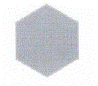
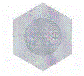
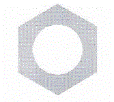
[0023] The second step is to make a regular hexagon with a radius of 7.5 microns as the inscribed circle, and expand it outward, such as 0.4 microns (such as figure 1 ); make the required small circle in it, the diameter of the small circle is 10 microns (such as figure 2 ); make a logical subtraction of the two (under the LEDIT software environment, select the two to execute the subtract command) (such as image 3 );

[0024] The third step is to move 7.5 microns in the X direction of the coordinates and 12.99 microns in the Y direction according to the regular triangle arrangement, forming a ...


PUM

PropertyMeasurementUnit
diameteraaaaaaaaaa

Abstract

The invention relates to a data split method and a correction method of a stepping photoetching mask plate for a diagrammed substrate manufacturing process. The method comprises the following processes of: determining the size and the space size of small circles on the photoetching mask plate; determining the edge length of a regular triangle distributed by the small circles and setting the edge length as a; making a regular hexagon which takes 1 / 2a as the radius of an incircle and expanding the regular hexagon outwards; making the small circles needed in the regular hexagon and carrying out logic reduction operation on the small circles and the regular hexagon; according to the regular-triangle distribution mode, moving for 1 / 2a in the X direction of the coordinate and for a*sin600 in the Y direction, forming a two-hexagon regular hexagon diagram, and repeatedly distributing the two-hexagon regular hexagon diagram, wherein the stepping is a, 2a*sin600; obtaining the needed window diagram shown in the abstract and the drawings; carrying out centering processing on the obtained window diagram; and adding an overlaid mark of the stepping photoetching machine with the corresponding type. The invention has the advantages that an exposure window interface obtained after repeated distribution is of a regular gear shape or a sawtooth shape, so that the split mode on the circle is effectively avoided, the optical edge effect is greatly improved and simultaneously the accuracy requirement for manufacturing the photoetching mask plate is reduced.

Description

technical field [0001] The invention discloses a high-quality PSS (Pattern Sapphire Substrate, PSS) manufacturing process stepping photolithography mask plate (referred to as PSS plate) data splicing method and correction method, generally speaking, it is a method for stepping photolithography The engraving machine uses the data splicing method and correction method in the design process of the high-precision and high-yield photolithography mask plate that does not increase the requirements. This photolithography plate is mainly used in the PSS manufacturing process. Background technique [0002] Due to the high requirements of the PSS version - high precision and high yield. However, when making a mask for a stepper lithography machine, there are obvious optical edge effects, and there are obvious errors at the edge of the window pattern; when using a stepper lithography machine for lithography exposure, the steps in the X and Y directions The advance and verticality requi...

Claims


Application Information

Patent Timeline
Patent Type & Authority Patents(China)
IPC IPC(8): G03F1/36
Inventor 叶红王玉林袁卓颖毛臻琪王刚明
Owner NO 55 INST CHINA ELECTRONIC SCI & TECHNOLOGYGROUP CO LTD
Why Eureka
Try Eureka