Gate-oxidizing-layer interface-trap density-testing structure and testing method

A technology of testing structure and interface traps, which is applied in the direction of single semiconductor device testing, semiconductor/solid-state device components, semiconductor devices, etc., can solve the problems of high test cost, long measurement time, low test efficiency, etc., to shorten the measurement time, Effects of area saving and test equipment cost saving

Active Publication Date: 2012-06-27
PEKING UNIV
View PDF3 Cites 20 Cited by
  • Summary
  • Abstract
  • Description
  • Claims
  • Application Information

AI Technical Summary

Problems solved by technology

Using this test structure and method for the interface trap density of the gate oxide layer, the measurement time is long, the test efficiency is low, and the test cost is high.

Method used


Image

  • Gate-oxidizing-layer interface-trap density-testing structure and testing method
  • Gate-oxidizing-layer interface-trap density-testing structure and testing method
  • Gate-oxidizing-layer interface-trap density-testing structure and testing method

Examples


Embodiment Construction

[0027] The specific implementation manners of the present invention will be further described in detail below in conjunction with the accompanying drawings and embodiments. The following examples are used to illustrate the present invention, but are not intended to limit the scope of the present invention.

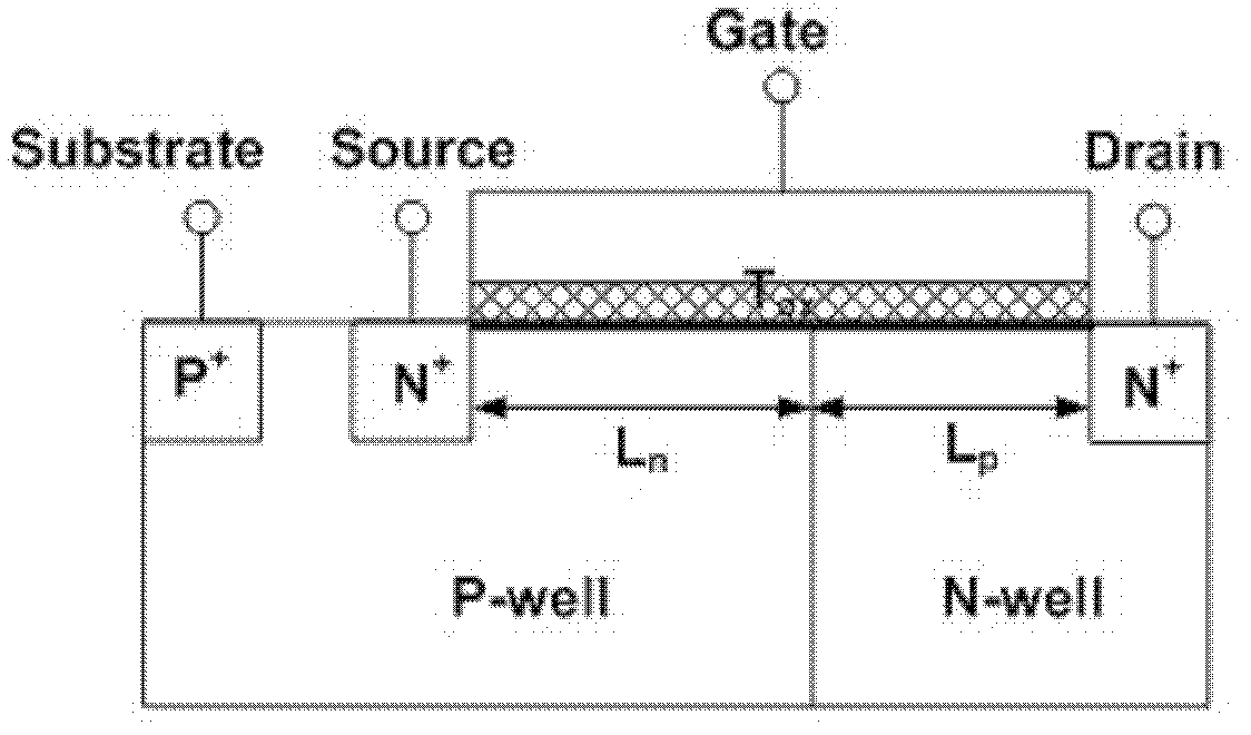
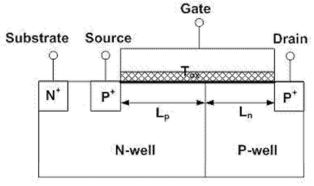
[0028] The invention provides a gate oxide layer interface trap density test structure, including n-type MOSFET and corresponding p-type gate oxide layer capacitance, or p-type MOSFET and corresponding n-type gate oxide layer capacitance; the n-type MOSFET and its corresponding The p-type gate oxide layer capacitance of the p-type MOSFET and its corresponding n-type gate oxide layer capacitor share the gate. Wherein, one side of the test structure is an n-type MOSFET, its n+ doping constitutes the source of the test structure, its p+ doping and p well region constitute the substrate of the test structure, and its gate constitutes the A part of the gate of the test structu...


PUM


Abstract

The invention discloses a gate-oxidizing-layer interface-trap density-testing structure and testing method, which relates to the technical field of the quality and reliability testing for MOS (Metal Oxide Semiconductor) devices. The testing structure comprises an n-type MOSFET (Metal-Oxide-Semiconductor Field Effect Transistor) and a corresponding p-type gate-oxidizing-layer capacitor or a p-type MOSFET and a corresponding n-type gate-oxidizing-layer capacitor; and the n-type MOSFET and the corresponding p-type gate-oxidizing-layer capacitor or the p-type MOSFET and the corresponding n-type gate-oxidizing-layer capacitor are shared with a grid electrode. The testing for the gate-oxidizing-layer interface-trap density of n-type and p-type MOS devices can be finished by adopting the same testing structure according to the invention, so that the measuring time is shortened, the testing efficiency is improved, and the testing cost is lowered.

Description

technical field [0001] The invention relates to the technical field of MOS device quality and reliability testing, in particular to a gate oxide layer interface trap density testing structure and testing method. Background technique [0002] With the rapid development of semiconductor technology and the substantial increase in the integration of microelectronic chips, the design and processing level of integrated circuits has entered the nano-MOS era. As the core of MOS devices, the gate oxide layer plays a decisive role in the quality and reliability evaluation of MOS devices. The role of the interface trap density of the gate oxide layer is one of the very important indicators. The generation of traps at the interface of the gate oxide reduces the mobility of the device, leading to a decrease in the performance of the device. Therefore, it is very necessary to monitor the traps at the interface of the gate oxide in the process flow, and a considerable number of sample test...

Claims


Application Information

Patent Timeline
Patent Type & Authority Applications(China)
IPC IPC(8): H01L23/544G01R31/26
CPCH01L2924/0002H01L2924/00
Inventor 何燕冬洪杰张钢刚张兴
Owner PEKING UNIV
Why Eureka
Try Eureka