Microcomponent vacuum packaging method

A technology for vacuum packaging and micro-devices, which is applied to electric solid-state devices, semiconductor devices, micro-structure devices, etc., can solve the problems of reducing packaging efficiency, taking a long time, and increasing the volume of devices, achieving a simple and effective packaging method and saving packaging costs. , to achieve the effect of electrical connection

Active Publication Date: 2015-02-18
XIAMEN UNIV
View PDF7 Cites 0 Cited by
  • Summary
  • Abstract
  • Description
  • Claims
  • Application Information

AI Technical Summary

Problems solved by technology

The above three bonding methods can be applied to wafer-level packaging, but it is difficult to lead out the electrodes required by the device, which is not conducive to subsequent device testing
Glass paste bonding can be applied to wafer-level packaging, which can encapsulate most materials and does not require high surface quality. However, if glass paste is used for direct packaging, organic solvents are likely to remain in the packaging cavity, which will affect the long-term performance of the device. stability
At present, the device-level packaging technology of MEMS devices is relatively mature. Usually, ceramic shells and metal shells are used to package a single device. The packaging process is relatively complicated and time-consuming, and the packaging cost accounts for 50% to 80% of the entire device cost.
Druck uses glass tubes to vacuum-package pressure sensors. The length of the glass tube is more than 1cm, which causes a serious increase in the volume of the packaged device, and requires large-scale equipment such as flame fusion glass and device support fixtures, and packages individual devices one by one. packaging efficiency

Method used


Image

  • Microcomponent vacuum packaging method
  • Microcomponent vacuum packaging method
  • Microcomponent vacuum packaging method

Examples


Embodiment Construction

[0028] The present invention comprises the following steps:

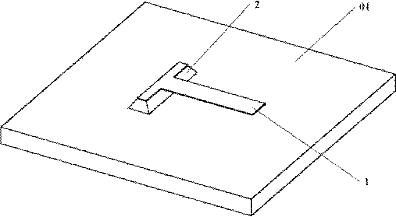
[0029] see figure 1 , using micromachining technology to process on the lower silicon wafer 01 such as figure 1 The silicon island 2 shown, the MEMS movable structure 1 and the attached metal electrodes and leads;

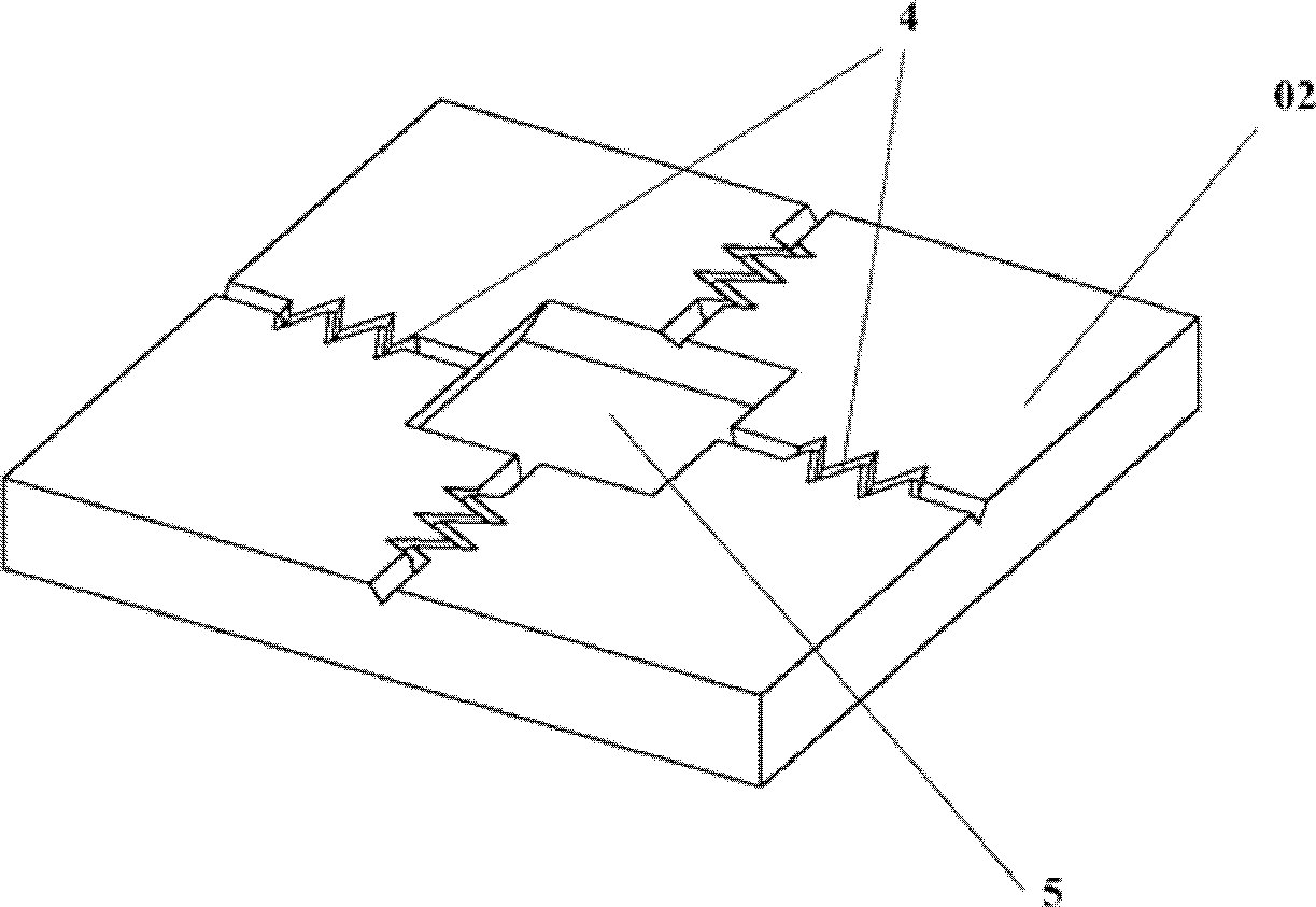
[0030] see figure 2 , through anisotropic wet etching of the silicon wafer, a trapezoidal through hole 5 is etched on the front side of the upper silicon wafer 02. When the glass paste is bonded, the movable mechanism 1 is placed in the trapezoidal through hole 5; The size of the flow channel 4 is on the order of microns, and the shape of the micro flow channel 4 is in the form of an "S" broken line, which is made by wet etching or ICP dry etching technology;

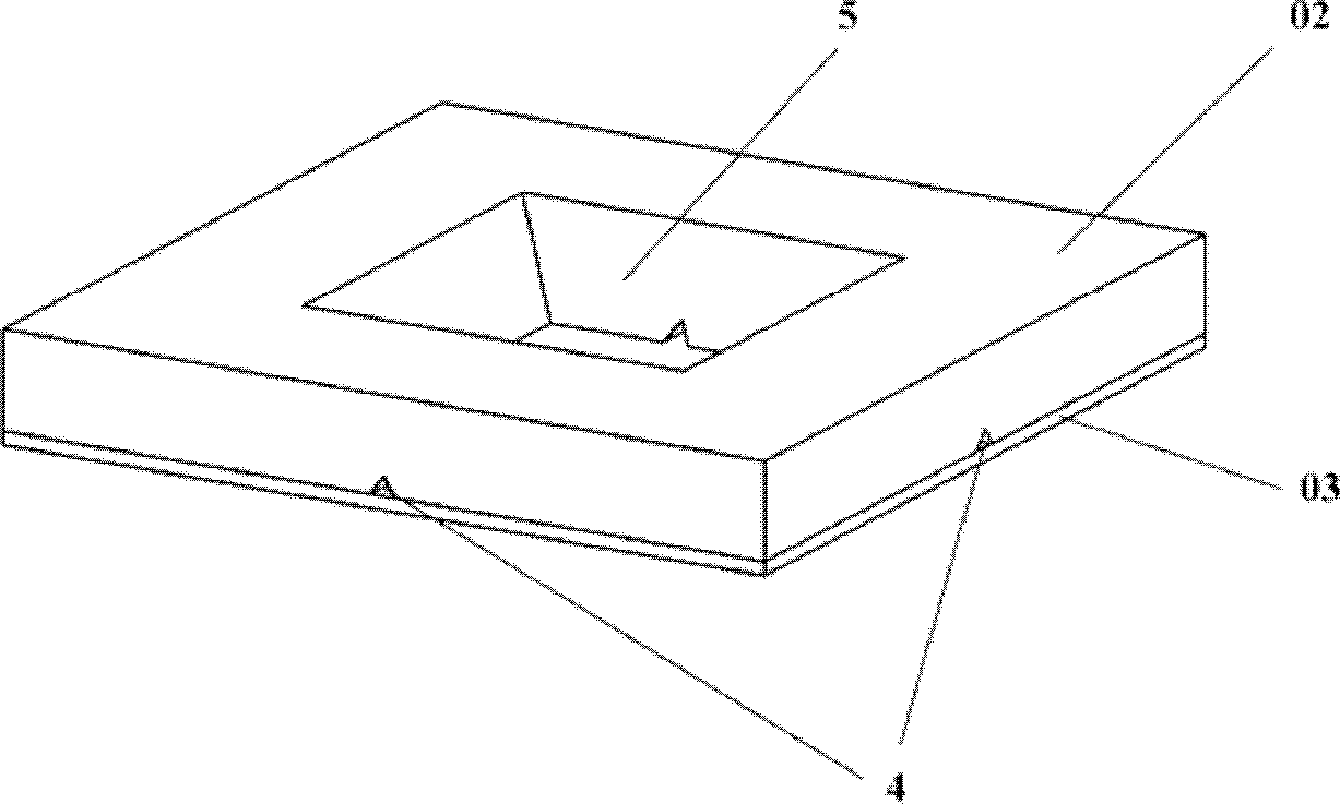
[0031] see image 3 , the cover plate 03 is made of 7740 glass, and the upper silicon wafer 02 and the glass cover plate 03 are bonded together by anodic bonding technology;

[0032] see Figure 4~6 , the front of the upper silicon wafer 02...


PUM


Abstract

A microcomponent vacuum packaging method relates to a microcomponent packaging method. A micro processing technology is adopted to process a silicon island, a movable structure, an auxiliary metal electrode and a lead on a lower silicon chip, wherein a wet etching method is adopted, a trapezoid through hole is processed in the front side of an upper silicon chip, and a micro runner is processed at the back side of the upper silicon chip; a silicon-glass anodic bonding technology is adopted to bond the silicon chip with a glass cover plate together; a glass size bonding technology is adopted to bond the upper and the lower silicon chips; and the bonded round pieces are placed in the vacuum bonder, gases in a cavity body can be sucked by the micro runner, a laser localized heating technology is adopted to partially smelt the glass cover plate, the molten glass seals the micro rubber, the wafer level vacuum packing of micro-electro-mechanical systems (MEMS) components is finally realized.

Description

technical field [0001] The invention relates to a packaging method for micro devices, in particular to a vacuum packaging method for micro-electromechanical (MEMS) devices using micro-channel laser local heating technology, which can be used for packaging resonant pressure sensors, micro gyroscopes, etc. Tiny devices in a highly airtight vacuum environment. Background technique [0002] MEMS technology is mainly used to make micro-sensors, micro-electronics, micro-actuators and micro-structures. After years of development, the design and manufacturing technology of MEMS devices has been quite mature, but many chips have not been practically used as products, the main reason is that the packaging problem has not been solved. MEMS vacuum packaging is a packaging technology that uses a sealed cavity to provide a highly airtight vacuum environment. Vacuum packaging enables the movable parts of MEMS devices to work in a vacuum environment, which greatly improves the quality fact...

Claims


Application Information

Patent Timeline
Patent Type & Authority Patents(China)
IPC IPC(8): B81C1/00B81B7/00
Inventor 王凌云吕文龙杜晓辉苏源哲占瞻左文佳孙道恒
Owner XIAMEN UNIV
Why Eureka
Try Eureka