Production method of nitrogen-free dielectric antireflective film

A production method and anti-reflection technology, applied in the manufacture of circuits, electrical components, semiconductors/solid-state devices, etc., can solve the problem of poor photoresist shape, inability to effectively eliminate photoresist standing wave effect and photoresist poisoning effect, and difficult to control Nitrogen-free dielectric anti-reflection film reflectivity extinction coefficient and other issues, to achieve the effect of controlling reflectivity and extinction coefficient, eliminating standing wave effect of photoresist, and eliminating poisoning effect of photoresist

Inactive Publication Date: 2012-07-04
SHANGHAI HUALI MICROELECTRONICS CORP
View PDF5 Cites 0 Cited by
  • Summary
  • Abstract
  • Description
  • Claims
  • Application Information

AI Technical Summary

Problems solved by technology

[0003] The deposition thickness of the nitrogen-free dielectric antireflection film is generally about several hundred angstroms (for example, 200-500 angstroms), and the whole deposition process is usually only a short ten seconds. If there is no time delay between the reactive gas and the plasma on, it is difficult to control the reflectance (RI) and extinction coefficient (K) of the resulting nitrogen-free dielectric antireflective film, which can lead to poor shape of the photoresist and cannot Effectively eliminate photoresist standing wave effect and photoresist poisoning effect

Method used


Image

  • Production method of nitrogen-free dielectric antireflective film
  • Production method of nitrogen-free dielectric antireflective film
  • Production method of nitrogen-free dielectric antireflective film

Examples


Embodiment Construction

[0020] In order to make the above objects, features and advantages of the present invention more comprehensible, specific implementations of the present invention will be described in detail below in conjunction with the accompanying drawings.

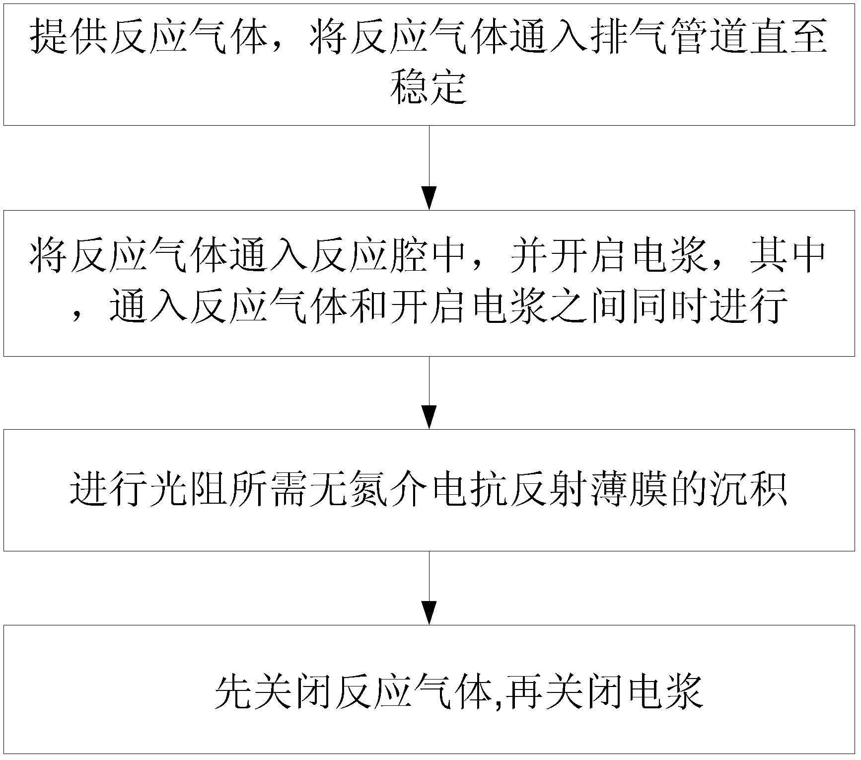
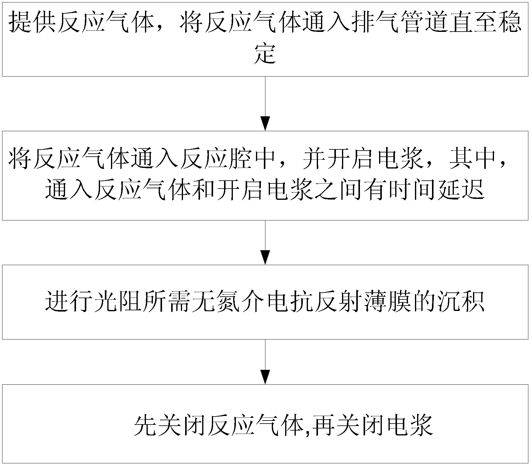
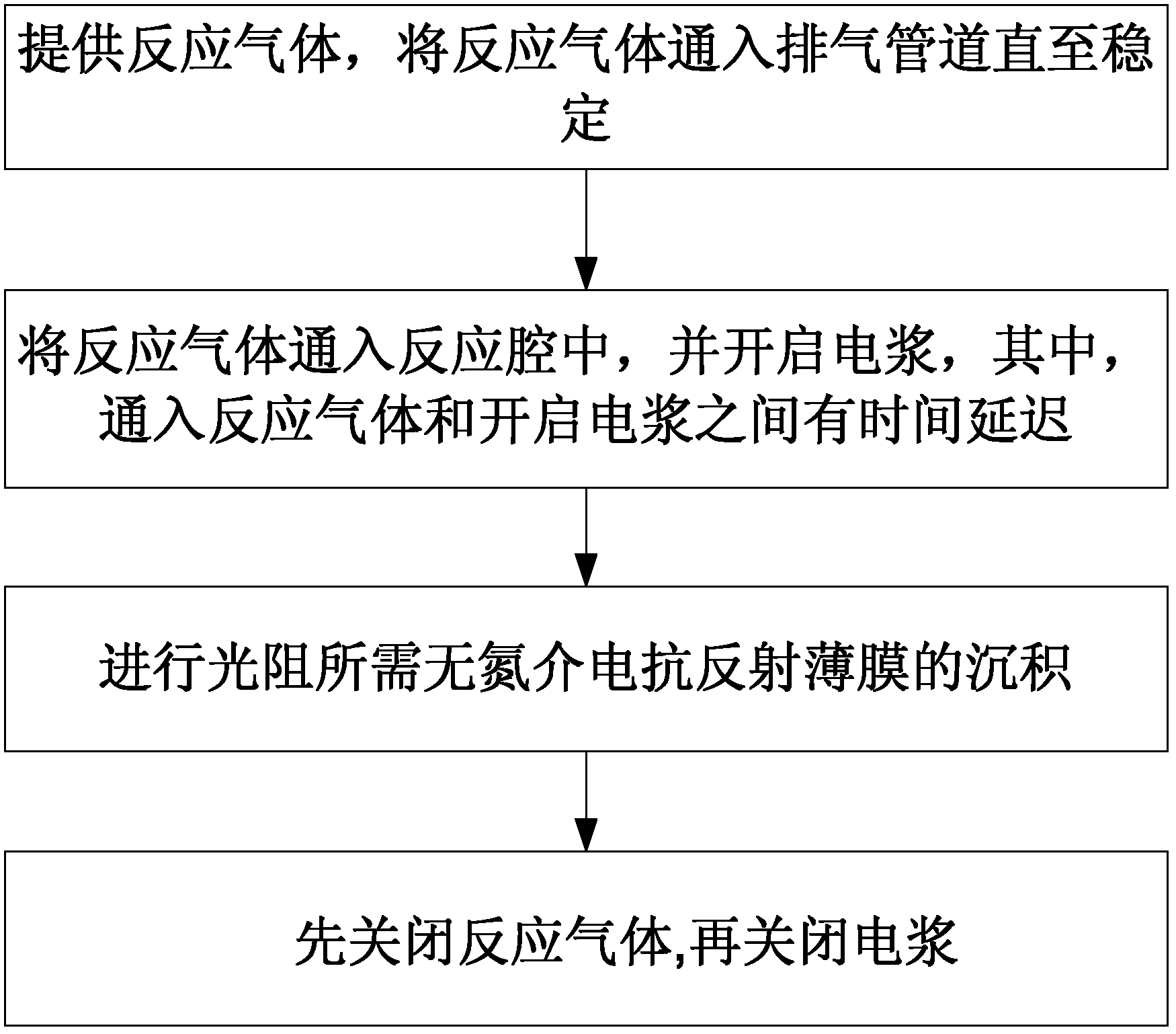
[0021] Such as figure 2 Shown, the manufacture method of the nitrogen-free dielectric antireflective film of an embodiment of the present invention, comprises the steps:

[0022] Firstly, a reactive gas is provided, which is a mixed gas of silane and carbon dioxide, and helium or other inert gas can also be used as an auxiliary gas.

[0023] Next, the above-mentioned reaction gas is passed into the exhaust pipe, and the flow rate of the reaction gas is kept stable;

[0024] Next, the above-mentioned reaction gas is passed into the reaction chamber, and the plasma is turned on. There is a certain time delay between passing the reaction gas and turning on the plasma. Preferably, the time delay is between 0.1 second and 2 seconds. When...


PUM

PropertyMeasurementUnit
thicknessaaaaaaaaaa
reflectanceaaaaaaaaaa

Abstract

The invention discloses a production method of a nitrogen-free dielectric antireflective film. The method comprises the following steps of: introducing a reactant gas into an exhaust pipe until the reaction is steady, introducing the reactant gas into a reaction chamber, and then starting the plasma; or, firstly starting the plasma, and then, introducing the reactant gas into the reaction chamber; finishing deposition of the nitrogen-free dielectric antireflective film by making use of the time delay between introducing the reactant gas and starting the plasma; and finally, closing the reactant gas, and then, closing the plasma. The production method of the invention can effectively control the reflectivity and the extinction coefficient of the nitrogen-free dielectric antireflective film, get a straighter light resistance shape and greatly eliminating the light resistance standing wave effect and the light resistance poisoning effect.

Description

technical field [0001] The invention relates to the field of semiconductor manufacturing, in particular to a method for manufacturing a nitrogen-free dielectric antireflection film. Background technique [0002] In the prior art, the manufacturing method of the nitrogen-free dielectric anti-reflection film adopts the simultaneous opening of the plasma and the passage of the reaction gas. Such as figure 1 Shown, the manufacture method of the nitrogen-free dielectric anti-reflection film (Nitrogen free DARL) of prior art comprises the steps: first, provide reaction gas; Then, reaction gas is passed into exhaust pipe until stable; Then, react The gas is passed into the reaction chamber, and the plasma is turned on at the same time. In this step, there is no time delay between passing the reaction gas and turning on the plasma, so as to complete the deposition of the nitrogen-free dielectric antireflection film; finally, the reaction gas is turned off first, Then turn off the ...

Claims


Application Information

Patent Timeline
Patent Type & Authority Applications(China)
IPC IPC(8): H01L21/314
CPCC23C16/50C23C16/45512
Inventor 陈建维张旭升
Owner SHANGHAI HUALI MICROELECTRONICS CORP
Why Eureka
Try Eureka