Table-board manufacture technology for lead-free diode

A lead-free diode and manufacturing process technology, applied in semiconductor/solid-state device manufacturing, electrical components, circuits, etc., can solve problems such as numerous process steps and product breakage, and achieve the effect of reducing the pickling process

Inactive Publication Date: 2012-07-04
如皋市日鑫电子有限公司
View PDF2 Cites 1 Cited by
  • Summary
  • Abstract
  • Description
  • Claims
  • Application Information

AI Technical Summary

Problems solved by technology

[0002] At present, the traditional process of etching the chip mesa of single-chip diodes is pickling. The disadvantage of this process is that the acid reacts with the lead-free solder and causes the product to break.
Our company has also developed a process of alkali and acid mixed corrosion to overcome the above shortcomings. The patent number of this process is 2009101346788, and the patent name is the mesa manufacturing process of lead-free diodes. However, the disadvantage of this method is two-step alkali corrosion Composed of acid corrosion, the process steps are relatively numerous

Method used


Image

  • Table-board manufacture technology for lead-free diode
  • Table-board manufacture technology for lead-free diode

Examples


Embodiment Construction

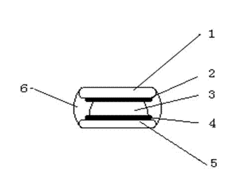
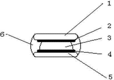
[0008] As shown in the figure, the diode is welded together by electrodes 1, soldering tabs 2, chips 3, soldering tabs 4, and electrodes 5. After welding, the two electrodes are sealed with silicone rubber or polyimide glue 6, and then placed on the The overall outer surface of its composition is encapsulated with epoxy resin.

[0009] The above chip mesa etching process is changed from traditional acid etching to alkali etching. The specific steps are as follows: there are two steps for mesa corrosion with a strong base, and the strong base used in the present invention is potassium hydroxide or sodium hydroxide solution. For the first mesa corrosion, the mass concentration of the strong alkali solution is: 8-15%, the corrosion temperature is 70-95°C, and the corrosion time for the chip mesa is 5-15 minutes; the concentration used for the second corrosion mesa is slightly lower The strong alkali solution is used for corrosion, the mass concentration of the strong alkali solu...


PUM


Abstract

The invention discloses a table-board manufacture technology for a lead-free diode. The table-board manufacture technology is characterized by corroding the table-board of the lead-free diode directly corroded twice by strong alkali; corroding for the first time by using strong alkali with mass concentration of 8-15% at 70-95 DEG C. for 5-15 minutes; and corroding second time using strong alkali with mass concentration of 2-6% at 70-95 DEG C. for 5-15 minutes. The table-board manufacture technology disclosed by the invention has the advantages that after the subsequent acid washing steps in patent 2009101346788 with a patent name of table-board manufacture technology for lead-free diode is reduced, the problem that products are broken by reaction of acid and lead-free welding sheets is solved, the high-temperature welding of the product is ensured at the speed of 265+ / -5 DEG C / 10s, and various performances can be equivalent to those of the table-board manufactured by the mentioned patent.

Description

technical field [0001] The invention relates to a mesa manufacturing process for lead-free diode chips, in particular to a mesa manufacturing process for integrated circuits, high-voltage silicon stacks, multi-chip and single-chip lead-free diodes with a melting point greater than 270°C. Background technique [0002] At present, the traditional process of etching the chip mesa of single-chip diodes is pickling. The disadvantage of this process is that the acid reacts with the lead-free solder to cause the product to break. Our company has also developed a process of alkali and acid mixed corrosion to overcome the above shortcomings. The patent number of this process is 2009101346788, and the patent name is the mesa manufacturing process of lead-free diodes. However, the disadvantage of this method is two-step alkali corrosion It is composed of acid corrosion, and the process steps are relatively numerous. Contents of the invention [0003] The main task of the present inv...

Claims


Application Information

Patent Timeline
Patent Type & Authority Applications(China)
IPC IPC(8): H01L21/329H01L21/306
Inventor 陆国华吴亚红陈炎
Owner 如皋市日鑫电子有限公司
Why Eureka
Try Eureka