Package and manufacture method for thermal enhanced quad flat no-lead flip chip

A four-sided flat, flip-chip technology, which is applied in the manufacture of semiconductor/solid-state devices, electrical components, and electrical solid-state devices, can solve the problem of low bonding strength between lead frame and plastic packaging material, lead frame and plastic packaging material falling off, and inability to lock effectively Solve problems such as plastic materials, achieve the effect of improving flip-chip welding quality and surface mount quality, improving cutting efficiency, and improving reliability

Inactive Publication Date: 2012-07-04
BEIJING UNIV OF TECH
View PDF4 Cites 29 Cited by
  • Summary
  • Abstract
  • Description
  • Claims
  • Application Information

AI Technical Summary

Problems solved by technology

The traditional lead frame has no step structure design, which cannot effectively lock the plastic material, resulting in low bonding strength between the lead frame and the plastic packaging material, which is easy to cause delamination of the lead frame and the plastic packaging material or even the falling off of the pin or chip carrier, and cannot effectively Prevent moisture from diffusing into the electronic package along the interface between the lead frame and the plastic packaging material, which seriously affects the reliability of the package
Traditional QFN products need to paste tape on the back of the lead frame in advance to prevent overflow during the plastic packaging process. After plastic packaging, cleaning processes such as removing the tape and molding compound flash need to be performed, which increases the packaging cost.
Use a dicing knife to cut and separate traditional quad flat no-lead packages. The dicing knife will also cut the lead frame metal while cutting the plastic packaging material, which will not only reduce the cutting efficiency and shorten the life of the dicing blade, but also produce metal burrs. , affecting the reliability of the package

Method used


Image

  • Package and manufacture method for thermal enhanced quad flat no-lead flip chip
  • Package and manufacture method for thermal enhanced quad flat no-lead flip chip
  • Package and manufacture method for thermal enhanced quad flat no-lead flip chip

Examples


Embodiment Construction

[0070] The present invention is described in detail below in conjunction with accompanying drawing:

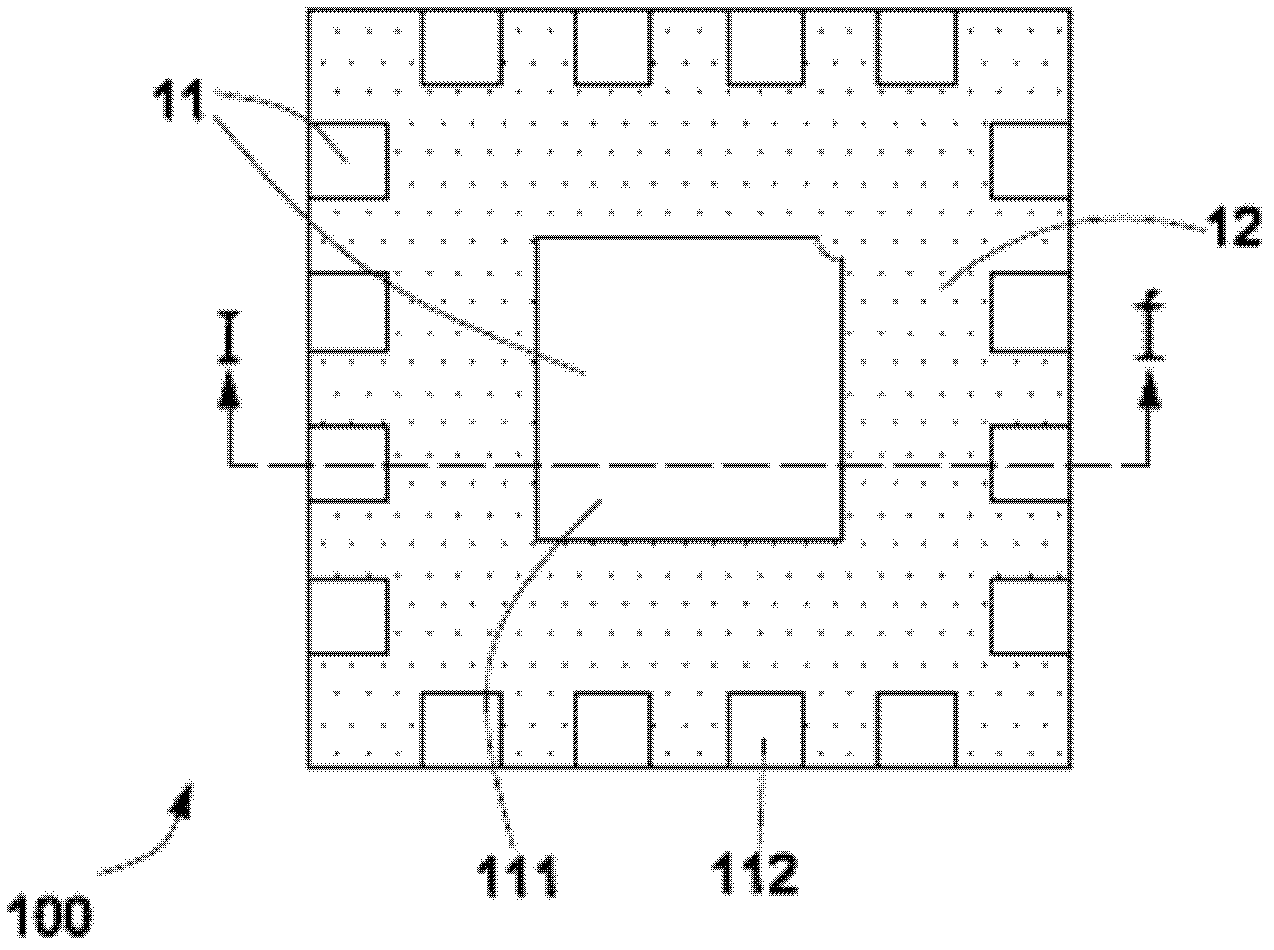
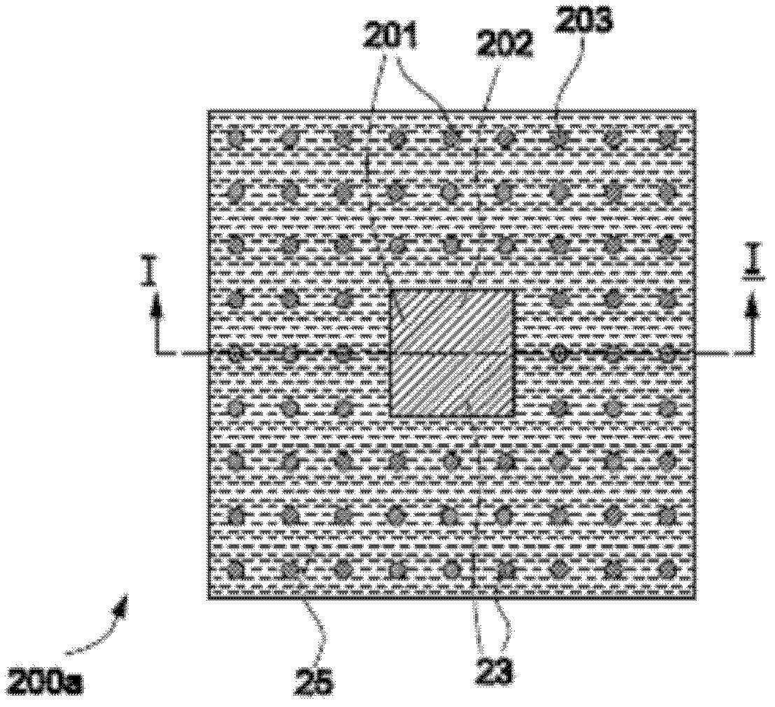
[0071] Figure 2A A schematic diagram of the back side of a heat-enhanced multi-turn pin arrangement FCQFN package structure drawn according to an embodiment of the present invention where the cross section of the pins is circular and the pins are arranged in parallel on each side of the chip carrier. Figure 2B A schematic diagram of the back side of a heat-enhanced multi-turn pin arrangement FCQFN package structure drawn according to an embodiment of the present invention in which the cross-section of the pins is rectangular and the pins are arranged in parallel on each side of the chip carrier.

[0072] Refer to the above Figure 2A -B It can be seen that, in this embodiment, the lead frame 201 of the heat-enhanced multi-turn pin arrangement FCQFN package structure 200a and 200b includes a chip carrier 202 and pins 203 arranged in multi-turn around the chip carrier 202, an...


PUM


Abstract

The invention discloses a packaging and manufacturing method for a thermal enhanced quad flat no-lead flip chip. A thermal enhanced quad flat no-lead flip chip package piece structure comprises a lead framework, a first metal material layer, a second metal material layer, IC chips with convex points, an insulating filler material, a sticking material, radiating fins, heat conducting spacers and a plastic package material, wherein the lead framework comprises a chip carrier and a plurality of pins arranged in multiple circles around the chip carrier; the first metal material layer and the second metal material layer are respectively configured on the upper surface and the lower surface of the lead framework; the IC chips with the convex points are invertedly welded and configured at the position of the first metal material on the upper surface of the lead framework; the insulating filler material is configured below the stepped structure of the lead framework; the heat conducting spacers are configured between the IC chips and the chip carrier through the sticking material; and the radiating fins are configured on the edgeless surfaces of the IC chips through the sticking material and wrapped by the plastic package material to form a package piece. The QFN (Quad Flat No-lead) package piece structure provided by the invention has the advantages of high reliability, low cost and high I/O (Input/Output) density.

Description

technical field [0001] The present invention relates to the technical field of manufacturing semiconductor components, and in particular to a heat-enhanced multi-turn pin arrangement four-sided flat non-lead flip-chip package (Flip Chip Quad Flat Non-lead Package, FCQFN), and the present invention also includes the package The manufacturing method of the parts. Background technique [0002] With the development of electronic products such as mobile phones and notebook computers towards miniaturization, portability, ultra-thinness, multimedia and low-cost requirements for popularization, high-density, high-performance, high-reliability and low-cost packaging forms and Its assembly technology has been developed rapidly. Compared with the expensive BGA and other packaging forms, the new packaging technology developed rapidly in recent years, that is, the quad flat non-lead QFN (Quad Flat Non-lead Package) package, due to its good thermal performance and electrical performance,...

Claims


Application Information

Patent Timeline
Patent Type & Authority Applications(China)
IPC IPC(8): H01L23/31H01L23/495H01L23/367H01L21/56
CPCH01L2224/32245H01L24/97H01L2224/97H01L2924/18161H01L2224/73265H01L2224/48247H01L2224/16245H01L2224/73253H01L2924/30107H01L2924/3011H01L24/73H01L2924/14
Inventor 秦飞夏国峰安彤武伟刘程艳朱文辉
Owner BEIJING UNIV OF TECH
Why Eureka
Try Eureka