Knot-free nanowire field effect transistor

A technology of field-effect transistors and nanowires, which is applied in semiconductor devices, electrical components, circuits, etc., can solve problems such as the difficulty of forming devices, and achieve increased on-state current, increased speed, and weakened leakage-induced barrier reduction effects. Effect

Inactive Publication Date: 2012-07-04
PEKING UNIV SHENZHEN GRADUATE SCHOOL +1
View PDF4 Cites 10 Cited by
  • Summary
  • Abstract
  • Description
  • Claims
  • Application Information

AI Technical Summary

Problems solved by technology

However, at the same time, the shrinkage of the device makes it difficult to form an obvious source-drain and channel barrier junction, and at a low concentration of channel doping concentration, the change of doping has a great impact on the performance of the device, so the junction-free nanometer The line field effect transistor came into being and attracted much attention
[0003] The current driving ability and transconductance of the existing junctionless nanowire field effect transistor can no longer meet the increasing demand, and it is necessary to make further structural improvements to improve the current driving ability of the device

Method used


Image

  • Knot-free nanowire field effect transistor
  • Knot-free nanowire field effect transistor
  • Knot-free nanowire field effect transistor

Examples


Embodiment Construction

[0025] In order to make the object, technical solution and advantages of the present invention clearer, the present invention will be further described in detail below in conjunction with the accompanying drawings and embodiments.

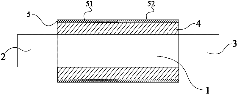
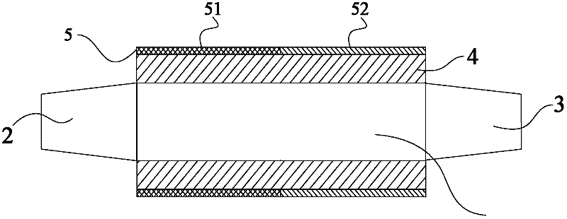
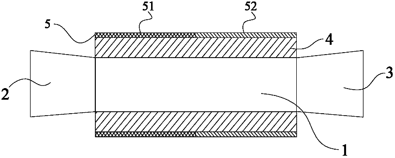
[0026] Please also refer to Figure 1 to Figure 4 as shown, Figure 1 to Figure 4 A cross-sectional schematic diagram of a junctionless nanowire field effect transistor provided for an embodiment of the present invention. In the figure, the junctionless nanowire field effect transistor includes a channel 1, a source region 2 and a drain region 3, and the source region 2 is arranged on the side of the channel 1. At one end, the drain region 3 is arranged at the other end of the channel 1 , the outer surface of the channel 1 is covered with a gate oxide layer 4 , and the surface of the gate oxide layer 4 is covered with a gate electrode layer 5 . In this embodiment, a split gate structure is introduced, and the gate electrode layer 5 includes a firs...


PUM


Abstract

The invention discloses a knot-free nanowire field effect transistor which comprises a channel, a source region and a drain region. The source region is arranged at one end of the channel, and the drain region is arranged at the other end of the channel; the outer surface of the channel is covered by a gate oxide layer which is covered by a grid electrode layer; and the grid electrode layer comprises a first grid electrode layer which is close to the source region and a second grid electrode layer which is close to the drain region. Compared with the prior art, the embodiment of the invention has the advantages that: by adopting a split gate structure, the speed of the charge carrier in the channel of the knot-free nanowire field effect transistor is increased, so the on-state current is increased, the off-state current of a device is reduced irrespective of the influence of the threshold voltage, the influence of the drain region on the device is screened, the drain induced barrier lowering effect is obviously weakened and the driving ability of the current is improved. Meanwhile, with the split gate, the transconductance feature of the knot-free nanowire field effect transistor under low voltage is obviously improved.

Description

technical field [0001] The invention belongs to the technical field of semiconductors, in particular to a split-ring gate junction-free nanowire field-effect transistor. Background technique [0002] The development of integrated circuits has been guided by Moore's Law, making integrated circuits higher density, lower power consumption, and more functions that can be realized, all of which are inseparable from device size reduction and performance improvement. However, with the continuous shrinking of the device size, especially when the device enters the deep nanoscale, various secondary effects of the device, such as short channel effect, leakage-induced barrier lowering effect, etc., lead to the degradation of device performance. Therefore, in order to suppress adverse effects such as short channels and improve device performance, many new device structures have been continuously proposed, such as double-gate devices, triple-gate devices, fin field effect transistors, and...

Claims


Application Information

Patent Timeline
Patent Type & Authority Applications(China)
IPC IPC(8): H01L29/423H01L29/78
Inventor 楼海君林信南何进
Owner PEKING UNIV SHENZHEN GRADUATE SCHOOL
Why Eureka
Try Eureka