Si-ge heterojunction NPN (negative-positive-negative) triode device and manufacturing method thereof

A heterojunction and triode technology, applied in semiconductor/solid-state device manufacturing, semiconductor devices, electrical components, etc., can solve the problems of high cost, complex deep trench isolation process, and high cost of epitaxy in the collector area, and achieve cost savings, process Simple, effect of reducing device size

Active Publication Date: 2012-07-04
SHANGHAI HUAHONG GRACE SEMICON MFG CORP
View PDF4 Cites 2 Cited by
  • Summary
  • Abstract
  • Description
  • Claims
  • Application Information

AI Technical Summary

Problems solved by technology

The device technology is mature and reliable, but the main disadvantages are: 1. The epitaxy cost of the collector area is high; 3. The deep trench isolation process is complicated and the cost is high

Method used


Image

  • Si-ge heterojunction NPN (negative-positive-negative) triode device and manufacturing method thereof
  • Si-ge heterojunction NPN (negative-positive-negative) triode device and manufacturing method thereof
  • Si-ge heterojunction NPN (negative-positive-negative) triode device and manufacturing method thereof

Examples


Embodiment Construction

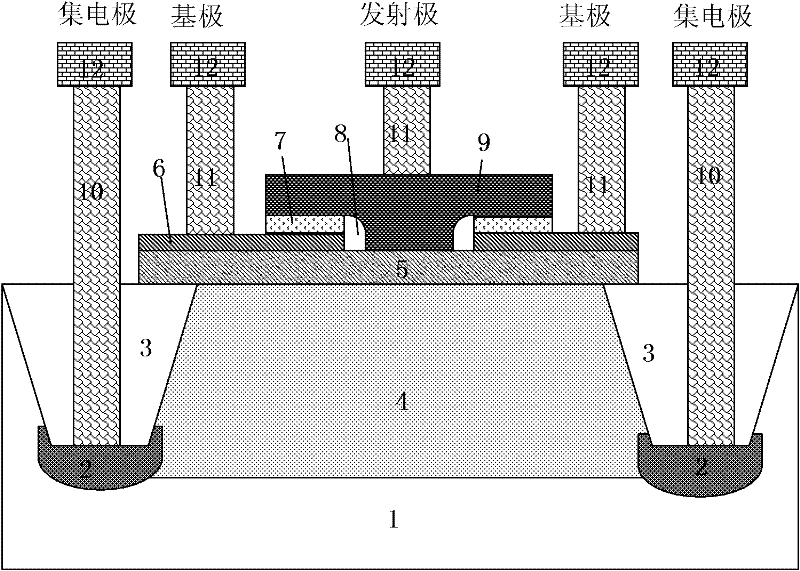
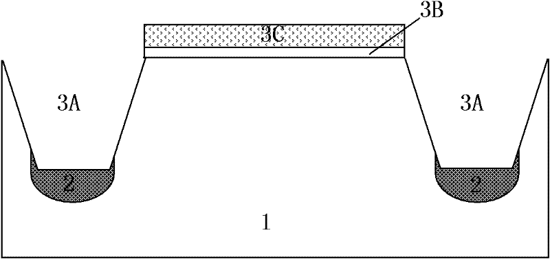
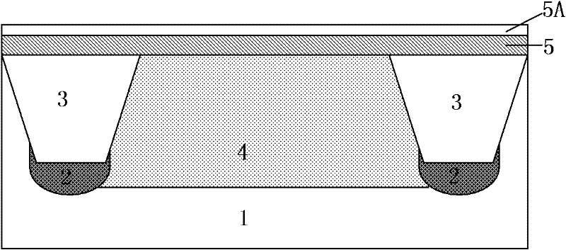
[0046] Such as figure 1 Shown is a schematic diagram of the structure of a germanium-silicon heterojunction NPN transistor device according to an embodiment of the present invention. The germanium-silicon heterojunction NPN transistor device according to an embodiment of the present invention is formed on a P-type silicon layer 6 substrate 1, and the active region is composed of a shallow trench field oxygen 3 isolation, the silicon-germanium heterojunction NPN triode device includes:

[0047] A collector region 4 is composed of an N-type ion implantation region formed in the active region, and the depth of the collector region 4 is greater than the depth of the bottom of the shallow trench field oxygen 3 . The N-type ion implantation process conditions of the collector region 4 are as follows: the implanted impurity is phosphorus or arsenic, the implantation energy is 50keV-500keV, and the implantation dose is 5e11cm -2 ~5e13cm -2 .

[0048] A pseudo-buried layer 2, which ...


PUM


Abstract

The invention discloses a si-ge heterojuncition NPN (negative-positive-negative) triode device, which comprises a collector area, an N-type buried layer, a P-type si-ge epitaxial layer, an emitter window, an intrinsic base area, an outer base area and an emitting area, wherein the collector area is formed in an active area and connected with the N-type pseudo buried layers formed at the bottom of shallow trench field oxygen of two sides of the active area, a collector electrode is guided out through deep hole contact, the emitter window is formed by etching P-type silicon and silicon nitride which are formed on the P-type si-ge epitaxial layer, the intrinsic base area is formed by the P-type si-ge epitaxial layer at the bottom of the emitter window, the outer base area is formed by the P-type si-ge epitaxial layer outside the emitter window and the P-type silicon, an inner side wall is formed on the inner wall of the window, and the emitting area is formed by N-type polycrystalline filled in the emitter window and extending to the outside of the window from the top. The invention further discloses a manufacturing method of the si-ge heterojunction NPN triode device. The size of the si-ge heterojunction NPN triode device and parasitic resistance of the collector electrode can be reduced, characteristic frequency of the device can be increased, process procedures can be simplified, process cost can be reduced and accurate control of process size can be realized.

Description

technical field [0001] The invention relates to the field of semiconductor integrated circuit manufacturing, in particular to a germanium-silicon heterojunction NPN transistor device; the invention also relates to a manufacturing method of the germanium-silicon heterojunction NPN transistor device. Background technique [0002] In radio frequency applications, higher and higher device characteristic frequencies are required. Although RFCMOS can achieve higher frequencies in advanced process technologies, it is still difficult to fully meet radio frequency requirements. For example, it is difficult to achieve characteristic frequencies above 40GHz, and advanced technology The research and development cost of compound semiconductors is also very high; compound semiconductors can realize very high characteristic frequency devices, but due to the disadvantages of high material cost and small size, and the toxicity of most compound semiconductors, its application is limited. Sili...

Claims


Application Information

Patent Timeline
Patent Type & Authority Applications(China)
IPC IPC(8): H01L29/737H01L29/06H01L29/08H01L29/417H01L21/331
Inventor 梅绍宁钱文生段文婷刘冬华胡君
Owner SHANGHAI HUAHONG GRACE SEMICON MFG CORP
Why Eureka
Try Eureka