
High-linearity frequency mixer in radio frequency identification
A high linearity, radio frequency identification technology, applied in electrical components, modulation transfer, demodulation and other directions, can solve problems such as linearity deterioration, and achieve the effect of increasing conversion gain and improving the ability to handle large signals
- Summary
- Abstract
- Description
- Claims
- Application Information
AI Technical Summary
Problems solved by technology
Method used
Image

Examples
Embodiment Construction
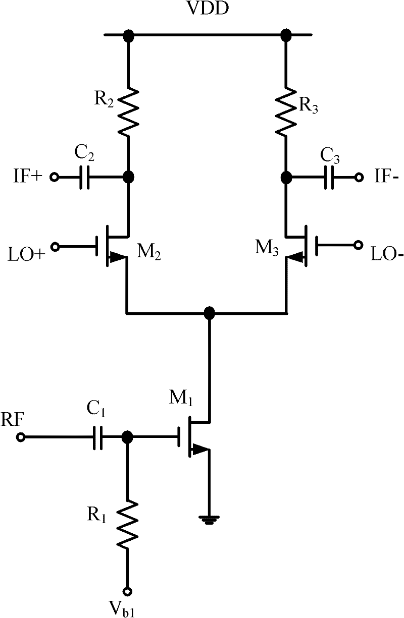
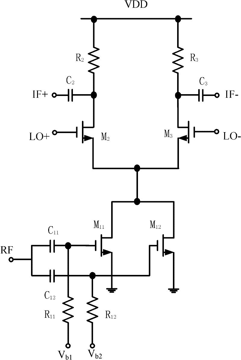
[0019] like figure 2 Shown is the circuit diagram of the high linearity mixer in the radio frequency identification of the embodiment of the present invention. The embodiment of the invention includes a load circuit, a switch circuit and a transconductance circuit. The load circuit and the switch circuit and as figure 1 The circuit structure of the conventional Gilbert mixer shown is the same. The following only describes the transconductance circuit of the embodiment of the present invention. The transconductance circuit of the embodiment of the present invention includes a first NMOS transistor M 11 , the second NMOS tube M 12 , the first input DC blocking capacitor C 11 , the first bias resistor R 11 , The second input DC blocking capacitor C 12 , the second bias resistor R 12 .
[0020] The first NMOS transistor M 11 and the second NMOS transistor M 12 The source of the ground, the first NMOS transistor M11 and the second NMOS transistor M 12 The drains of the...
PUM
 Abstract
Description
Claims
Application Information