Method for determining and testing ohmic contact between black silicon material and metal electrode

A metal electrode and ohmic contact technology, which is applied in the direction of measuring electricity, measuring devices, measuring electrical variables, etc., can solve the problems that the I-V characteristics of metal/black silicon materials cannot be directly tested, and achieve effective judgment, easy operation, and accurate ratio contact The effect of resistance

Inactive Publication Date: 2012-07-11
UNIV OF ELECTRONICS SCI & TECH OF CHINA
View PDF4 Cites 7 Cited by
  • Summary
  • Abstract
  • Description
  • Claims
  • Application Information

AI Technical Summary

Problems solved by technology

[0016] The invention provides a method for judging and testing ohmic contact between a black silicon material and a metal electrode to solve the problem that the I-V characteristics of the metal / black silicon material cannot be directly tested due to the existence of black silicon / single crystal silicon heterogeneity

Method used


Image

  • Method for determining and testing ohmic contact between black silicon material and metal electrode
  • Method for determining and testing ohmic contact between black silicon material and metal electrode
  • Method for determining and testing ohmic contact between black silicon material and metal electrode

Examples


Embodiment Construction

[0038] In order to make the object, technical solution and advantages of the present invention clearer, the present invention will be further described in detail below in conjunction with specific embodiments and with reference to the accompanying drawings.

[0039] The method for judging and testing the ohmic contact between the black silicon material and the metal electrode comprises the following steps:

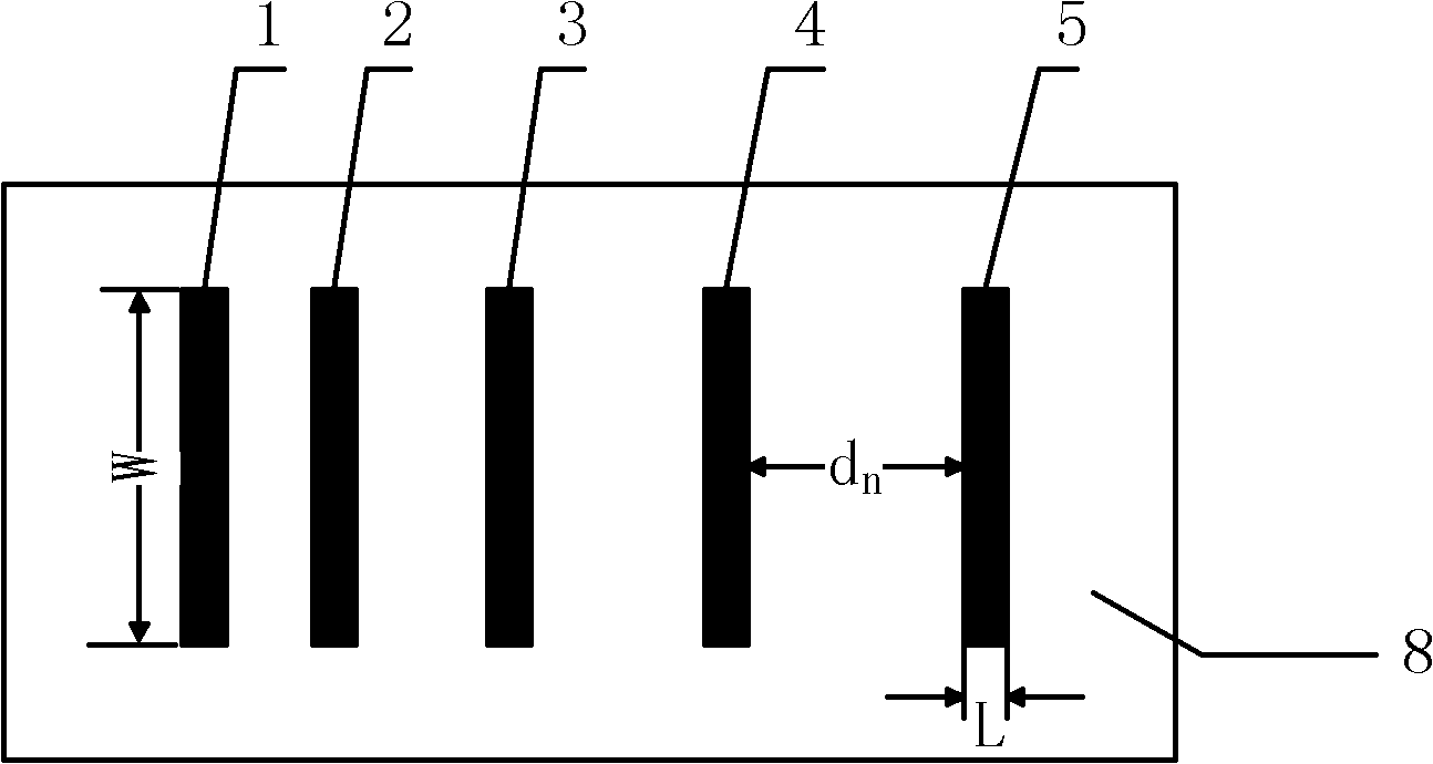
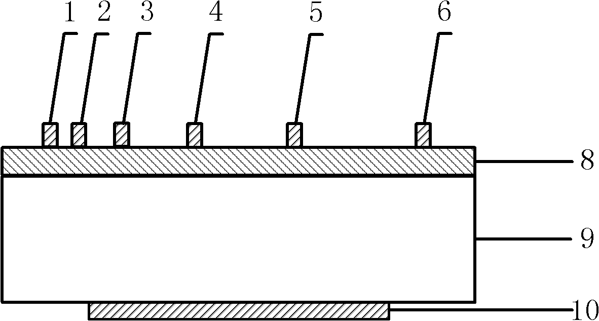
[0040] Step 1: If figure 2 As shown, three square Al / Ni electrodes 1, 2, 3 are prepared on the surface of the black silicon material 8, the electrode size is 2.0mm×2.0mm, and the spacing is 2.0mm. An Al electrode 10 is deposited on the back of the crystalline silicon 9, and the size of the electrode is 10.0 mm×10.0 mm.

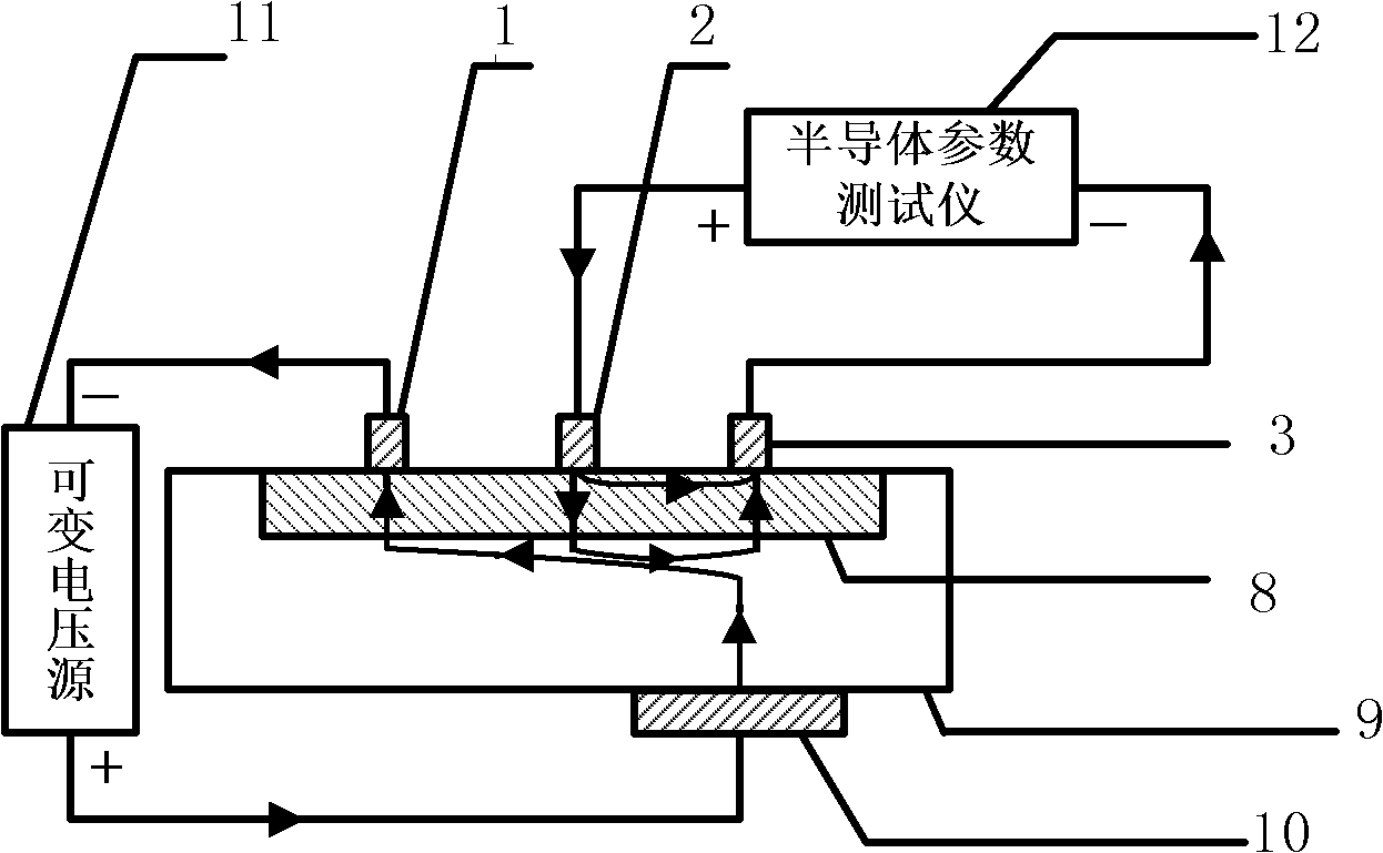
[0041] Step 2: Using the semiconductor parameter tester 12, apply a forward voltage bias of 2V between the electrodes 2 and 3, and test the current intensity between the two electrodes.

[0042] Step 3: Use a variable voltage source to apply a reverse vol...


PUM


Abstract

The invention discloses a method for determining and testing ohmic contact between a black silicon material and a metal electrode, belonging to the technical field of semiconductor photoelectronic materials and devices. The invention has the technical schemes that: an I-V characteristic curve of a metal / black silicon material can be directly tested through a three-electrode horizontal test device with a reverse bias voltage, and the contact type between the black silicon material and the metal electrode can be judged; and 2, the ohmic contact of the black silicon material can be tested by using a TLM (Transmission Line Model) method with the reverse bias voltage, thus a specific contact resistance can be obtained. According to the method disclosed by the invention, the influence on the determination and the test for the ohmic contact of the black silicon material due to heterojunction structures of black silicon / monocrystalline silicon in the traditional metal / black silicon / monocrystalline silicon sandwich structure is solved, and the specific contact resistance value of the metal / black silicon can be accurately tested.

Description

technical field [0001] The invention belongs to the technical field of semiconductor optoelectronic materials and devices, in particular to a method for judging and testing ohmic contact between black silicon materials and metal electrodes. Background technique [0002] Black silicon is a silicon material obtained when the research group of Professor Mazur of Harvard University uses a femtosecond laser to irradiate the surface of a single crystal silicon wafer in a certain gas environment. The surface of the obtained black silicon material contains quasi-regularly arranged micron-scale pyramid structures, and has a high-concentration chalcogen (oxygen) atom doping layer. Experiments have proved that the black silicon material absorbs almost all light with a wavelength of 250-2500nm, and it is extremely sensitive to incident light. Compared with photodetectors based on traditional silicon wafers, the sensitivity of black silicon wafers to light can be increased by 100~ 500 t...

Claims


Application Information

Patent Timeline
Patent Type & Authority Applications(China)
IPC IPC(8): G01R31/00G01R27/14
Inventor 李伟李雨励何敏赵国栋李世彬吴志明蒋亚东
Owner UNIV OF ELECTRONICS SCI & TECH OF CHINA
Why Eureka
Try Eureka