
Method for implementing dual-switch grid-control TWT (Traveling Wave Tube) modulator with high pulse repetition frequency and low power consumption on basis of MOS (Metal Oxide Semiconductor) tube

A technology of MOS tubes and implementation methods, which is applied in the field of electric vacuum tube grid-controlled modulators, can solve the problems of complex peripheral circuits of switching tubes, and achieve the effects of low power consumption, simplified circuits, and reliable operation

Active Publication Date: 2012-07-11
THE 724TH RES INST OF CHINA SHIPBUILDING IND
View PDF3 Cites 5 Cited by
  • Summary
  • Abstract
  • Description
  • Claims
  • Application Information

AI Technical Summary

Problems solved by technology

Due to the limitation of withstand voltage, the switch tube is used in series by several bipolar transistors or IGBTs, and the required voltage equalization circuit and isolated drive circuit make the peripheral circuit of the switch tube more complicated.

Method used


Image

  • Method for implementing dual-switch grid-control TWT (Traveling Wave Tube) modulator with high pulse repetition frequency and low power consumption on basis of MOS (Metal Oxide Semiconductor) tube
  • Method for implementing dual-switch grid-control TWT (Traveling Wave Tube) modulator with high pulse repetition frequency and low power consumption on basis of MOS (Metal Oxide Semiconductor) tube
  • Method for implementing dual-switch grid-control TWT (Traveling Wave Tube) modulator with high pulse repetition frequency and low power consumption on basis of MOS (Metal Oxide Semiconductor) tube

Examples


Embodiment Construction

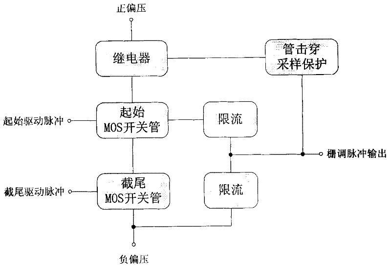
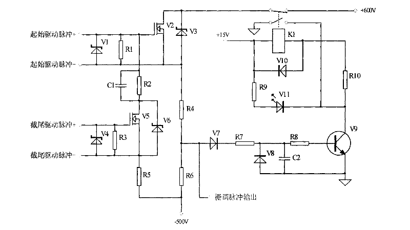
[0010] see figure 2 , the initial drive pulse drives the MOS transistor V2 to conduct, and the positive bias voltage of 600V is applied to the gate of the traveling wave tube through V2, K1, and R4. Resistor R4 is a positive bias current limiting resistor, and the value of R4 should not be large, otherwise it will affect the leading edge characteristics of the grid modulation pulse. The type of V2 is IXBH16N170, a MOS tube with a withstand voltage of 1700V; V3 is a transient suppression diode with a value of 1200V, which acts as an overvoltage protection for V2.

[0011] The truncated drive pulse drives the MOS transistor V5 to turn on, pulls the gate voltage of V2 to a low level forcibly, and turns off V2. At this time, the negative bias voltage of 500V rapidly charges the capacitance in the grid interspace of the traveling wave tube to the negative bias value through the conduction loop of V5. Resistor R5 acts as a current limiter, and choosing appropriate values ​​of C1,...


PUM


Abstract

The invention relates to a method for implementing a dual-switch grid-control TWT (Traveling Wave Tube) modulator with high pulse repetition frequency and low power consumption on the basis of a MOS (Metal Oxide Semiconductor) tube. In a conventional dual-switch grid-control modulator circuit, the high inverse-voltage MOS tube with good high frequency switching characteristic is used as a switching device, so that a modulator has good pulse front edge when a narrow pulse is output; a conventional mode of forming an oppositely-pulling state by short-time direct connection of start and end switching tubes so as to reduce time of a grid-modulated pulse back edge is changed and the loss on the switching tubes of the modulator is greatly reduced, so that the modulator can stably and reliably work under the extremely high repetition frequency; the single high inverse-voltage MOS tube is basically suitable for the voltage withstanding requirement and a voltage equalizing circuit and an isolating driving circuit are saved so that a circuit is simplified; and a TWT protection circuit is arranged so as to prevent a positive bias from being always added on a TWT grid when the start switching tube is broken down. The invention provides an effective technological approach for implementing the grid-control modulator with high performance and low power consumption and developing a grid-control TWT transmitter with high pulse repetition frequency.

Description

technical field [0001] The invention belongs to the electric vacuum tube grid-controlled modulator technology, and is a method for realizing a high-repetition-frequency, low-power-consumption double-switch grid-controlled traveling wave tube modulator based on MOS tubes. Background technique [0002] With the continuous development of the grid-controlled traveling wave tube transmitter in the direction of high repetition frequency and wide pulse width, it also puts forward higher requirements for the modulator, which must not only meet the working requirements of high repetition frequency and wide pulse width, but also Reduce the modulator's own loss to improve the reliability of the modulator and transmitter. [0003] The double-switch gate-controlled modulator is the most commonly used gate-controlled TWT modulator. The front and rear edges of the modulated pulse are separately controlled by the "start" and "truncated" switch tubes, so a smaller The leading and trailing e...

Claims


Application Information

Patent Timeline
IPC IPC(8): H01J23/00H01J25/34
Inventor 崔海安杨钰辉
Owner THE 724TH RES INST OF CHINA SHIPBUILDING IND
Learn More