Hermetic package method and structure of transistor base and transistor pin

A technology of hermetic packaging and transistors, which is applied in the direction of electrical components, electrical solid devices, semiconductor devices, etc., can solve the problems of silver-copper solder blocking the suspension hole, unstable production quality, and difficulty in plugging, and reduce cost consumption , The processing technology is simple and reasonable, and the effect of solving the blockage

Inactive Publication Date: 2012-07-11
CHINA ZHENHUA GRP YONGGUANG ELECTRONICS CO LTD STATE OWNED NO 873 FACTORY
View PDF5 Cites 11 Cited by
  • Summary
  • Abstract
  • Description
  • Claims
  • Application Information

AI Technical Summary

Problems solved by technology

When the fit gap is too large, weld material leakage will occur, which is not only difficult to achieve the plugging effect, but also its silver-copper solder will often block the suspension hole after brazing; It is difficult to assemble, and at the same time, the copper base plate will be slightly deformed after brazing, which will cause the bottom surface of the component kovar tube to protrude from the lower plane of the tube seat, thus affecting the quality of the product
Therefore, the existing hermetic packaging method of the transistor base and pins not only has the problems of high processing precision and high production cost, but also has the problems of difficult operation and unstable production quality.

Method used


Image

  • Hermetic package method and structure of transistor base and transistor pin
  • Hermetic package method and structure of transistor base and transistor pin

Examples


Embodiment Construction

[0010] The present invention will be further described in detail below in conjunction with the accompanying drawings and embodiments.

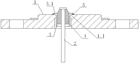
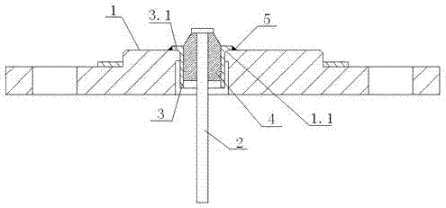
[0011] Embodiments of the present invention: a method for hermetically sealing transistor bases and pins according to the present invention is to make the pins 2 on the pins 2 in advance when the pins 2 of the transistor are fixed on the metal base 1 of the transistor. The glass insulator assembly composed of welding sleeve 3 and glass insulating layer 4, when manufacturing welding sleeve 3, a circle of flanging 3.1 is made on one end port of welding sleeve 3 at the same time, and its welding sleeve 3 can be made of metal materials, but It is preferably made of copper or copper alloy material in the prior art, and the pin 1 made of the glass insulator assembly is inserted into the pin hole of the metal tube base 1, and the flange 3.1 of the welding sleeve 3 is connected to the metal tube The seat 1 is in contact with each other, and then the w...


PUM


Abstract

The invention discloses a hermetic package method and structure of a transistor base and a transistor pin. According to the invention, when a transistor pin (2) of a transistor is fixed on a metal transistor base (1) of the transistor, and a glass insulator assembly which is composed of a welding sleeve (3) and a glass insulation layer (4) is made on the transistor pin (2) in advance; when the welding sleeve (3) is made, a circle of flange (3.1) is also made on the port of one end of the welding sleeve (3), and a transistor pin (2) with the glass insulator assembly is inserted in a transistor pin hole of the metal transistor base (1), the flange (3.1) of the welding sleeve (3) is in contact with the metal transistor base (1), and than the welding sleeve (3) and the metal transistor base (1) are welded together on the flange (3.1) of the welding sleeve (3) in a brazing manner. The hermetic package method and structure provided by the invention have the advantages of convenience for operation, good production quality, low cost, low processing accuracy requirement, high production efficiency, good product quality and the like.

Description

technical field [0001] The invention relates to a hermetic packaging method and structure of a transistor base and pins, and belongs to the technical field of semiconductor transistor production. Background technique [0002] The hermetic packaging of metal stems and pins of semiconductor transistors is an important technology to ensure the isolation of chips in the cavity of semiconductor devices from harmful atmospheres such as moisture and oxygen in the atmosphere. This technology can better ensure the performance of semiconductor devices. At present, in the prior art, the straight cylindrical sealing technology is often used to hermetically seal the metal socket and the pin. The straight cylindrical sealing technology is to first burn the glass insulator assembly on the pin, and then The glass insulator assembly is brazed to the metal socket. The existing straight packaging technology mainly relies on the matching accuracy of the outer diameter of the welding sleeve on ...

Claims


Application Information

Patent Timeline
Patent Type & Authority Applications(China)
IPC IPC(8): H01L21/50H01L21/60H01L23/488H01L23/10
Inventor 杨正义刘宗永唐勇
Owner CHINA ZHENHUA GRP YONGGUANG ELECTRONICS CO LTD STATE OWNED NO 873 FACTORY
Why Eureka
Try Eureka