Terminal structure of splitting gate groove power modular operating system (MOS) device and manufacturing method thereof

A technology of MOS devices and terminal structures, applied in semiconductor/solid-state device manufacturing, semiconductor devices, electrical components, etc., can solve problems such as being susceptible to external influences, unfavorable device stability, etc., to reduce process steps and process difficulty, save masking Membrane times, device reliability improvement effect

Inactive Publication Date: 2012-07-11
HARBIN ENG UNIV
View PDF7 Cites 10 Cited by
  • Summary
  • Abstract
  • Description
  • Claims
  • Application Information

AI Technical Summary

Problems solved by technology

Its characteristics are: the terminal is composed of a series of deep grooves, and the polysilicon electrode is suspended in the terminal, so the P-region in the suspended electrode is easily affected by the outside world, which is not conducive to the stability of the device

Method used


Image

  • Terminal structure of splitting gate groove power modular operating system (MOS) device and manufacturing method thereof
  • Terminal structure of splitting gate groove power modular operating system (MOS) device and manufacturing method thereof
  • Terminal structure of splitting gate groove power modular operating system (MOS) device and manufacturing method thereof

Examples


Embodiment Construction

[0024] The present invention is described below in conjunction with accompanying drawing.

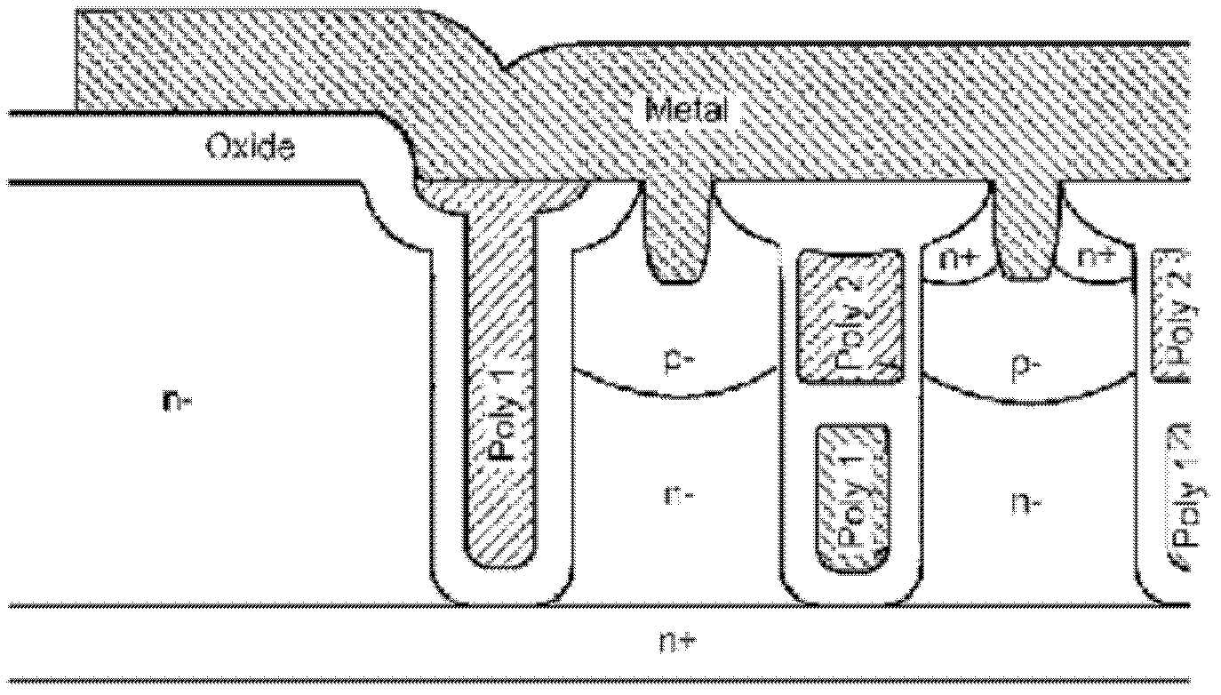
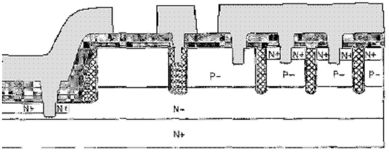
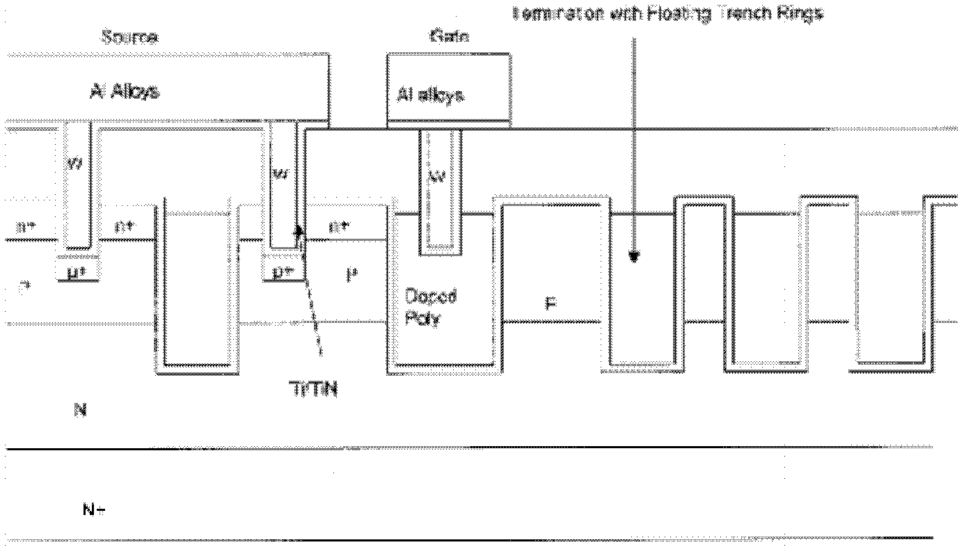
[0025] 1. In the terminal structure of the split gate trench power MOS device, the gate electrode lead-out structure and the corresponding lower split gate structure are produced under the same process conditions by the cells in the same device, as shown in the schematic diagram of the process steps in Figure 5 .

[0026] 2. The silicon nitride etched in Figure 5(e) is to ensure the gate lead-out electrode, because if the contact hole of the gate lead-out electrode is set in the gate electrode trench, it will be etched back by polysilicon when the gate electrode is formed The impact of the structure may affect the contact effect of the lightning contact. At the same time, the part of the gate extraction electrode is also used as a mask plate for N+ ion implantation to form the source electrode.

[0027] 3. The breakdown characteristic simulation curve of the split-gate trench MOSFET d...


PUM


Abstract

The invention provides a terminal structure of a splitting gate groove power modular operating system (MOS) device and a manufacturing method thereof. The terminal structure comprises a grid leading-out electrode (101), a grid electrode lower part suspended polycrystalline silicon electrode (102), a thick oxidized layer (103), grid electrode connecting metal (104), a source electrode (105), a floating area (N-) (106) and a drain electrode (107); and the grid electrode leading-out electrode (101), the grid electrode lower part suspended polycrystalline silicon electrode (102) and the thick oxidized layer (103) are assembled to form the device terminal and are formed through a same mask plate and same technique. The splitting gate groove power MOS device structure is realized through a process manufacturing flow of five photoetching plates, so the breakdown voltage and parasitic capacitance of the device are not influenced, while ultralow conducting resistance of the device can be guaranteed; and the production cost of the device can be reduced, while the process manufacturing flow is optimized.

Description

technical field [0001] The invention relates to a terminal structure of a split gate type trench power MOS device. The invention also relates to a method for manufacturing a terminal of a split-gate trench power MOS device. Background technique [0002] In the 1990s, the main research direction of the development of Power Trench MOSFET and industrialization technology was to minimize the forward conduction resistance (Ron) of low-voltage power devices. Today, the structure of power trench MOS devices is suitable for most power MOSFET applications, and the characteristics of the devices are constantly approaching the one-dimensional limit of silicon materials (expressing the characteristic on-resistance in the drift region of the device and the breakdown in the off-state Theoretical relationship of voltage). The proposal of REduced SURface Field (RESURF) technology can make power trench MOS devices with a breakdown voltage of 600V exceed the one-dimensional limit of silicon...

Claims


Application Information

Patent Timeline
Patent Type & Authority Applications(China)
IPC IPC(8): H01L29/78H01L29/423H01L21/336
CPCH01L29/407H01L29/66734H01L29/7811H01L29/7813
Inventor 王颖胡海帆焦文利曹菲
Owner HARBIN ENG UNIV
Why Eureka
Try Eureka