High thermal load large power semiconductor laser

A technology of semiconductors and lasers, which is applied in semiconductor lasers, lasers, laser components, etc., can solve problems such as poor stability, decreased optical coupling efficiency, and low optical power, and achieve reliability, good heat dissipation, and stability. Effect

Inactive Publication Date: 2012-07-11
STARWAY LASER
View PDF3 Cites 17 Cited by
  • Summary
  • Abstract
  • Description
  • Claims
  • Application Information

AI Technical Summary

Problems solved by technology

[0004] This C-mount packaging method, due to the structural limitation, the effective area of ​​the thermally conductive substrate 10 is small, and the area in contact with the heat sink is limited, resulting in a relatively small optical power, generally only below 8W
Moreover, since the semiconductor laser chip assembly can only be fixed on the heat sink by one screw, the stability is poor, and the position of the laser chip assembly is prone to change during use, which is easy to cause light in a micron-scale fiber coupling system. Coupling efficiency decreases, resulting in lower reliability of semiconductor lasers

Method used


Image

  • High thermal load large power semiconductor laser
  • High thermal load large power semiconductor laser
  • High thermal load large power semiconductor laser

Examples


Embodiment Construction

[0026] The preferred embodiment of the present invention will be described in detail below in conjunction with accompanying drawing:

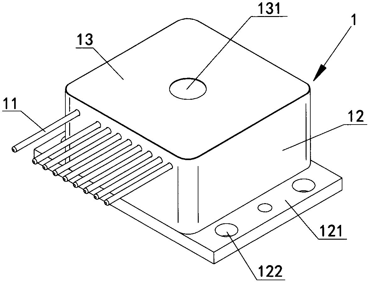
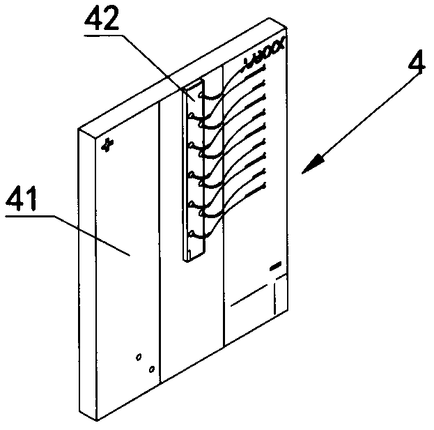
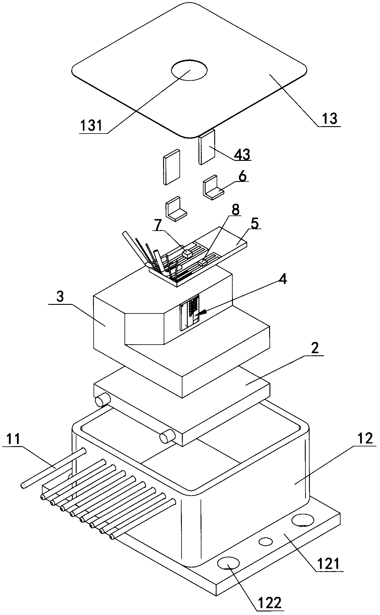
[0027] Such as figure 1 , image 3 and Figure 4 The shown semiconductor laser comprises a housing 1, a TEC refrigerator 2 arranged in the housing 1, a heat sink 3 fixed on the TEC refrigerator 2, a semiconductor laser chip assembly 4 pasted on the heat sink 3, and a For the drive circuit board 5 that realizes electro-optical conversion, the specific structural features of each part will be described below:

[0028] The housing 1 is mainly composed of a housing base 12 and a housing cover 13 closely fitted to the upper edge of the housing base 12 . In this embodiment, the housing 1 is in the shape of a cuboid as a whole, and a connecting wing 121 is extended from the bottom of the housing base 12, and a connecting hole 122 is provided on the connecting wing 121, through which the semiconductor laser is connected to the equipment to be insta...


PUM


Abstract

The invention relates to a high thermal load large power semiconductor laser which comprises a housing, a TEC refrigerator, a heat sink, a semiconductor laser chip assembly, and a circuit board. The semiconductor laser chip assembly is a chip assembly based on COS packaging and comprises a heat radiation substrate and a laser chip which is pasted on the heat radiation substrate. The heat radiation substrate is pasted on the heat sink. The circuit board is a circuit board whose metal surface is coated with ceramic, and the circuit board and the semiconductor laser chip assembly are electrically connected through a connecting copper sheet. The semiconductor laser has a good heat radiation effect, and manufacture of a large power laser can be realized. Simultaneously, the semiconductor laser chip is fixed with the heat sink by employing a pasting mode without deformation or displacement, influence on a product brought by change of machinery, temperature and the like can be overcome, and the reliability of the product is ensured.

Description

technical field [0001] The invention relates to a laser device, which can be used as a light source in systems such as optical communication, optical processing, and optical display. Background technique [0002] Semiconductor lasers develop rapidly due to the expansion of wavelength, the emergence of high-power laser arrays, and the emergence of compatible laser light guides and computer control of laser energy parameters. Semiconductor lasers are small in size, light in weight, low in cost, and have selectable wavelengths, and their application ranges are becoming wider and wider. [0003] Existing semiconductor lasers with high heat load are usually mainly composed of a tube shell, a refrigerator arranged in the tube shell, a heat sink, and a semiconductor laser chip assembly fixed on the heat sink. Among them, semiconductor laser chip components generally use C-mount packaging, such as Figure 5 shown. It includes a heat conduction substrate 10 , a laser chip 20 fixed ...

Claims


Application Information

Patent Timeline
Patent Type & Authority Applications(China)
IPC IPC(8): H01S5/024
Inventor 韩尧田国光李军凌勇孙松涛李琮马永坤徐连强
Owner STARWAY LASER
Why Eureka
Try Eureka