
Nanoscale resistance spot welding device and nanoscale resistance spot welding method

A resistance spot welding, nano-scale technology, applied in resistance welding equipment, nanotechnology, nanotechnology and other directions, can solve the problems of scrapped components, disconnected metal wires, unreliable connection strength, etc., to achieve simple operation and low cost. Effect

Inactive Publication Date: 2012-07-18
杭州轻巧科技有限公司
View PDF4 Cites 8 Cited by
  • Summary
  • Abstract
  • Description
  • Claims
  • Application Information

AI Technical Summary

Problems solved by technology

However, the connection between the nanowires obtained by this method is only achieved by the weak attraction of intermolecular contact, so the connection strength is not reliable.
[0004] On the other hand, due to the high integration of micro-nano devices, once a local defect or damage occurs during production and use, the entire component will be scrapped
The more common damage methods include disconnection of connection points, disconnection of metal wires, etc., and there is currently no effective way to repair them

Method used


Image

  • Nanoscale resistance spot welding device and nanoscale resistance spot welding method
  • Nanoscale resistance spot welding device and nanoscale resistance spot welding method
  • Nanoscale resistance spot welding device and nanoscale resistance spot welding method

Examples


Embodiment Construction

[0024] The present invention will be further described in detail below in conjunction with specific embodiments and accompanying drawings.

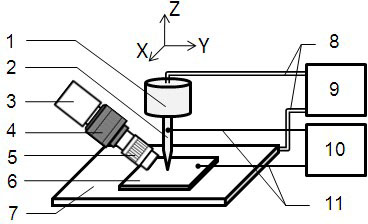
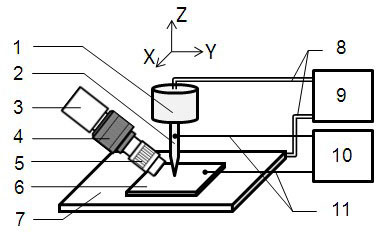
[0025] figure 1 The schematic diagram of the nanoscale resistance spot welding device is given. according to figure 1 , the nanoscale resistance spot welding device consists of scanning probe 2, CCD camera 3, zoom module 4, magnifying objective lens 5, scanning probe microscope control and feedback connection 8, scanning probe microscope control and feedback module 9 , The welding control power supply 10 and the welding power supply wire 11 are composed. The XYZ direction action module 1 moves the scanning probe 2 , and the processed workpiece 6 is fixed on the stage 7 .

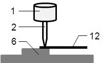
[0026] figure 2 An example of spot welding of a cantilever beam in a micro-nanoarchitecture is given. according to figure 2 As shown, the workpiece 6 to be processed is a silicon substrate with certain nanostructure protrusions, and its surface layer is evenly c...


PUM


Abstract

The invention belongs to the field of welding and material nano-machining, and particularly relates to a nanoscale resistance spot welding device and a nanoscale resistance spot welding method. The device comprises a high-power optical microscope, a scanning probe microscope, a welding control power supply and a welding connecting line, wherein the high-power optical microscope is used for primarily positioning a position to be welded of a machined workpiece and observing a welding process in real time, and the welding control power supply is used for supplying power needed in welding. The scanning probe microscope is used for accurately positioning and welding the position to be welded of the machined workpiece and comprises a conductive scanning probe, a control and feedback connecting line and a control and feedback module, wherein the scanning probe is capable of working in an accurately positioning mode and in a welding mode, and is respectively connected with the control and feedback module and the welding control power supply. The device and the method can be used for realizing nanoscale resistance spot welding, and have important significance for design and manufacture of novel micro-nano devices.

Description

technical field [0001] The invention belongs to the field of welding and material nano-processing, and in particular relates to a nanoscale resistance spot welding device and method. Background technique [0002] Micro-nano technology has been more and more widely used in people's daily life. The traditional processing method of micro-nano components, such as photolithography, adopts a top-down processing method, the basic principle of which is to transfer the shape structure on the photomask to the substrate surface through photochemical reaction, The steps of coating photoresist on the substrate, exposing, developing, etching, removing glue, etc. are obtained to obtain the micro-nano structure. This method has many steps and complex operations, and is basically only suitable for the preparation of planar micro-nano structures. For the micro-nano structure with three-dimensional structure, the photolithographic preparation method generally adopts the method of layer-by-la...

Claims


Application Information

Patent Timeline
Patent Type & Authority Applications(China)
IPC IPC(8): B23K11/11B23K11/36B82B3/00
Inventor 陈希章王建
Owner 杭州轻巧科技有限公司
Learn More