

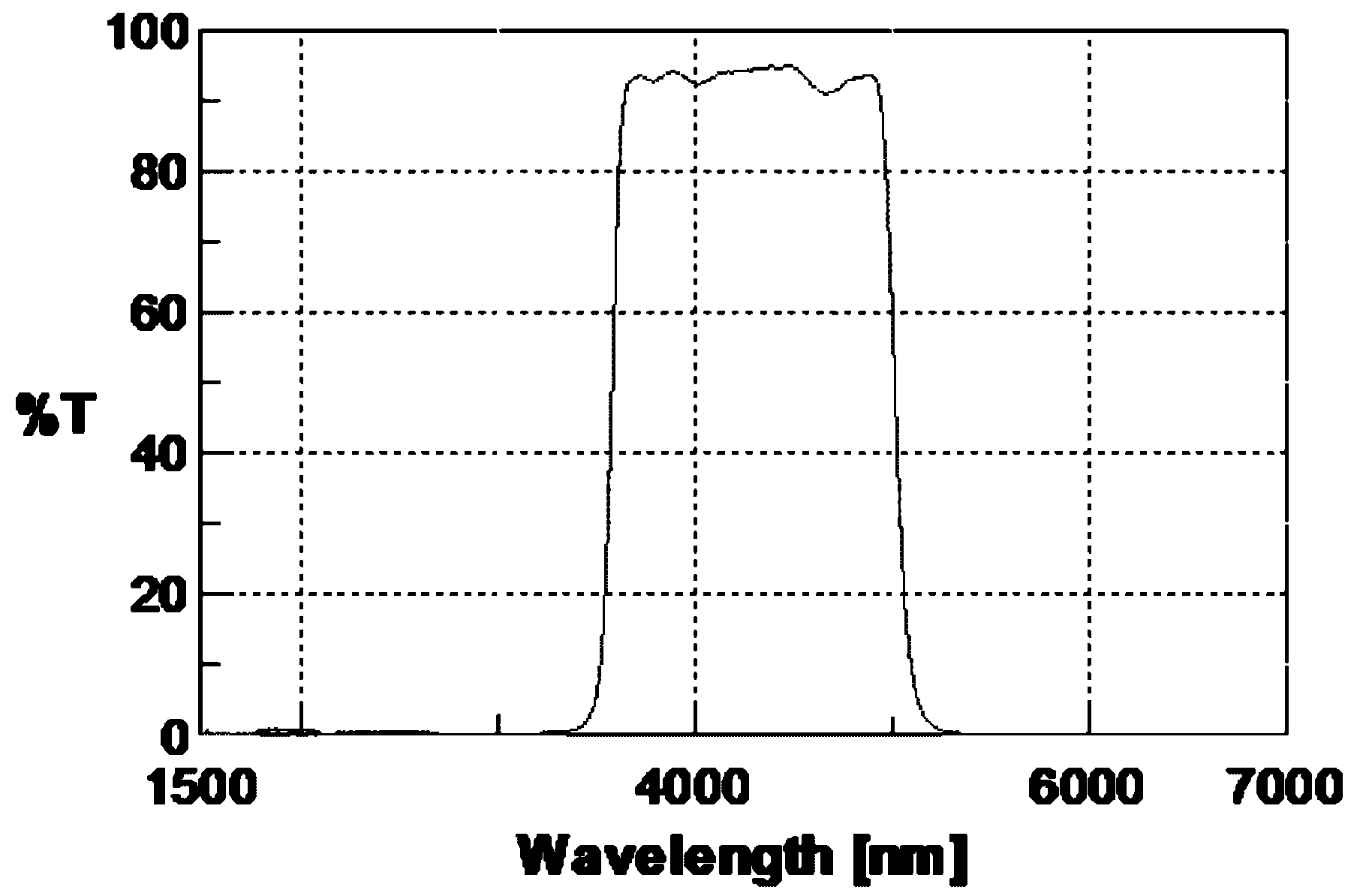
Infrared filter with broadband of 3.65 to 5 microns, and manufacturing method for infrared filter
A technology for an infrared filter and a manufacturing method, which are applied in the field of 3.65-micron to 5-micron broadband infrared filters and their manufacture, can solve the problems of poor precision and low signal-to-noise ratio, achieve excellent performance, and meet the requirements of sensitivity and precision , The effect of stable and mature process
- Summary
- Abstract
- Description
- Claims
- Application Information
AI Technical Summary
Problems solved by technology
Method used
Image


Examples
Embodiment 1
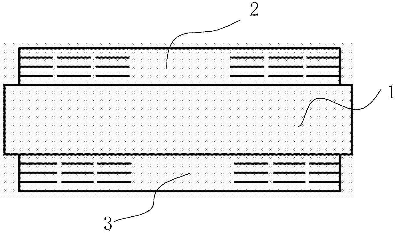
[0021] like figure 1 As shown, the present embodiment provides a 3.65 micron to 5 micron broadband infrared filter,
[0022] (1) Single-crystal germanium Ge with a size of Φ18×1.0mm is used as the substrate 1, the surface aperture N≤5, the local aperture ΔN≤0.5, the parallelism θ≤1', and the surface finish is better than 60 / 40;
[0023] (2) Silicon monoxide SiO and single crystal germanium Ge are selected as the coating material, and multi-layer interference films are respectively deposited on the two surfaces of the substrate;
[0024] (3) The design of the first mask series interference film 2: Sub|1.33(.5HL.5H)5 3.39(.5LH.5L)5|Air
[0025] The second mask is interference film 3. Design and use: Sub|0.92(.5HL.5H) 3 1.1(.5HL.5H) 4 |Air
[0026] The corresponding meanings in the film system are: Sub is the substrate, Air is air, H is λc / 4 single crystal germanium film, L is λc / 4 silicon monoxide film, λc=2μm, and the number in the structure is the thickness of the film l...
PUM
 Abstract
Description
Claims
Application Information