Nitride distributed Bragg reflector (DBR) and manufacturing method and application thereof

A Bragg mirror, distributed technology, applied in the field of optoelectronics, can solve the problems of poor crystal quality, insufficient smooth interface, cracking of epitaxial layer, etc., to achieve improved luminous efficiency, high crystal quality and interface smoothness, and growth rate is easy to adjust. Effect

Active Publication Date: 2014-12-03
山东鲁南大数据产业发展有限公司
View PDF8 Cites 0 Cited by
  • Summary
  • Abstract
  • Description
  • Claims
  • Application Information

AI Technical Summary

Problems solved by technology

Chinese patent document CN101478115A (CN200910110946.2) discloses a nitride distributed Bragg reflector (DBR) and its preparation method. The preparation method of the provided nitride DBR is to use aluminum nitride and gallium nitride on the gallium nitride buffer layer Alternately grown periodic structures are used to realize the DBR function. This method currently has great difficulties in growth. The lattice mismatch between aluminum nitride and gallium nitride makes it difficult to achieve the thickness and number of periods required by DBR. , DBR generally requires more than 20 cycles, using this method to grow DBR can easily lead to cracking of the epitaxial layer
If the same temperature is used to grow AlInN and GaN, it is easy to make the crystal quality of DBR deteriorate, the interface is not smooth enough, and it is difficult to achieve the effect of DBR

Method used


Image

  • Nitride distributed Bragg reflector (DBR) and manufacturing method and application thereof
  • Nitride distributed Bragg reflector (DBR) and manufacturing method and application thereof

Examples


Embodiment 1

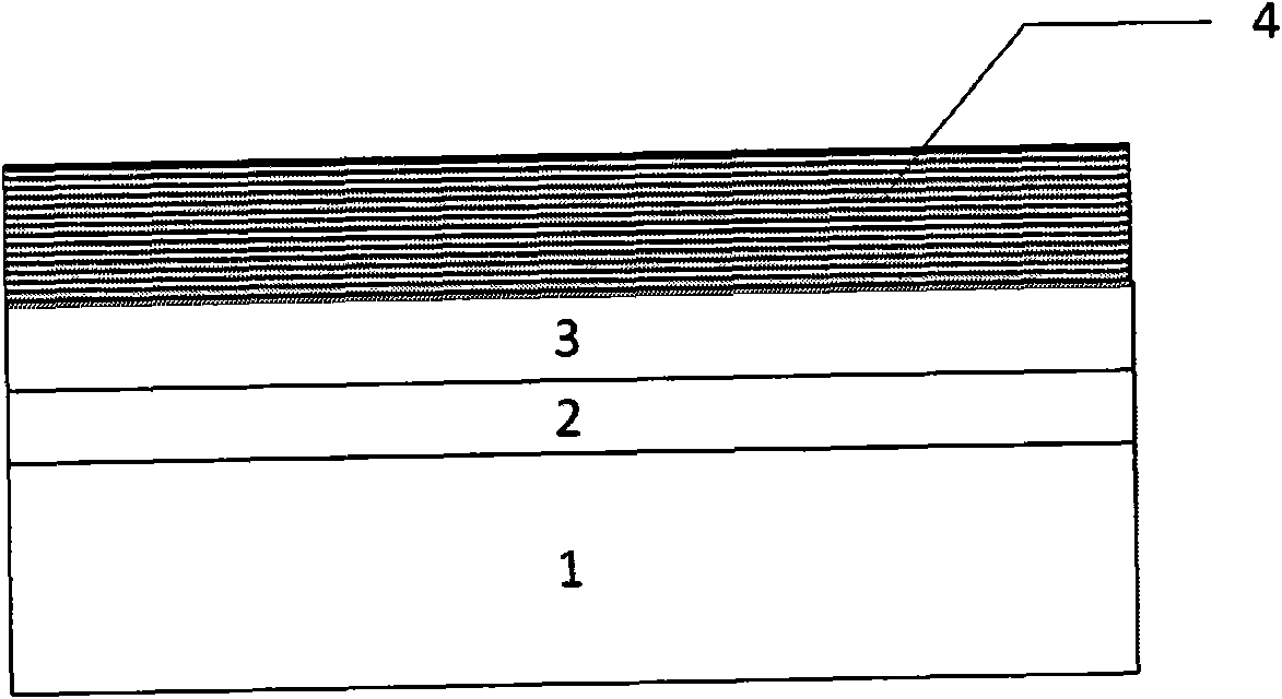
[0037] refer to figure 1 , to prepare Al on SiC substrates by metal-organic chemical vapor deposition x In y Ga 1-x-y N / Al u In v Ga 1-u-v Take the N-structure DBR as an example, including the following steps:

[0038] (1) The silicon carbide substrate 1 is placed in a reaction chamber of a metal organic chemical vapor deposition (MOCVD) furnace, heated to 1050° C. under a hydrogen atmosphere, and processed for 15 minutes.

[0039] (2) An aluminum nitride nucleation layer 2 is grown on a silicon carbide substrate 1 at a growth temperature of 1000° C., a thickness of 150 nm, and a growth pressure of 50 mbar.

[0040] (3) A non-doped gallium nitride layer (buffer layer) 3 is grown on the aluminum nitride nucleation layer 2 at a growth temperature of 1100° C., a growth thickness of 2 μm, and a growth rate of 2 μm / h.

[0041] (4) Al growth on the non-doped gallium nitride buffer layer 3 x In y Ga 1-x-y N / Al u In v Ga 1-u-v A distributed Bragg reflector (DBR structure) 4...

Embodiment 2

[0043] refer to figure 1 , to prepare Al on sapphire substrates by metal-organic chemical vapor deposition x In y Ga 1-x-y N / Al u In v Ga 1-u-v Take the N-structure DBR as an example, including the following steps:

[0044] (1) The sapphire substrate 1 is placed in the reaction chamber of a metal organic chemical vapor deposition furnace (MOCVD), heated to 1000° C. under a hydrogen atmosphere, and processed for 12 minutes.

[0045] (2) An AlGaN nucleation layer 2 is grown on a sapphire substrate 1 at a growth temperature of 900° C., a thickness of 120 nm, and a growth pressure of 70 mbar.

[0046] (3) A non-doped GaN layer 3 (buffer layer) is grown on the AlGaN nucleation layer 2 at a growth temperature of 1100° C., a growth thickness of 2 μm, and a growth rate of 2 μm / h.

[0047] (4) Al growth on the non-doped gallium nitride buffer layer 3 x In y Ga 1-x-y N / Al u In v Ga 1-u-v A distributed Bragg reflector 4 (DBR) composed of N quaternary structures, where x=0.3,...

Embodiment 3

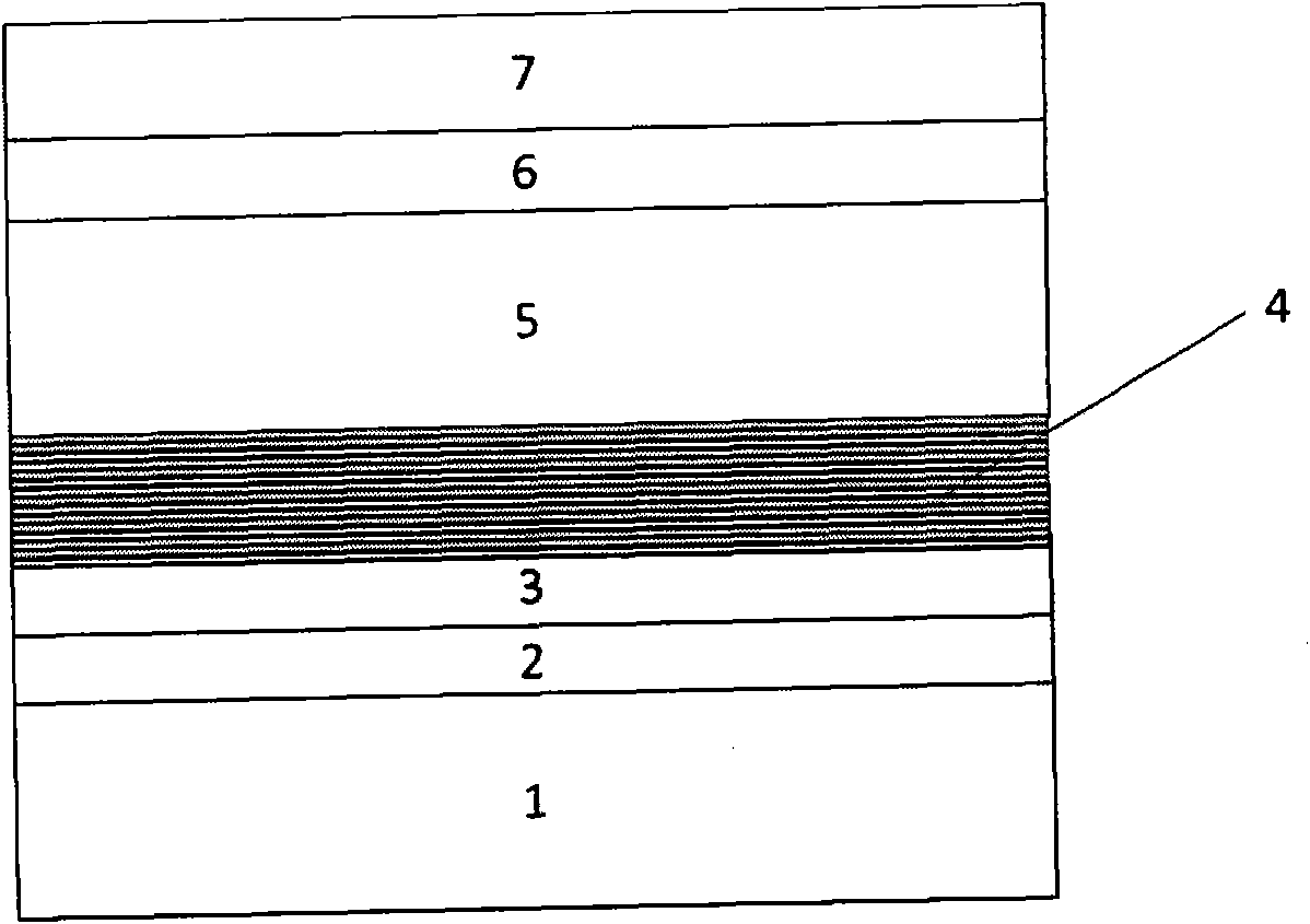
[0049] refer to figure 2 , taking the preparation of DBR-containing gallium nitride-based light-emitting diodes on a sapphire substrate as an example, the steps are as follows:

[0050] (1) The sapphire substrate 1 is placed in a reaction chamber of a metal organic chemical vapor deposition (MOCVD) furnace, heated to 1000° C. under a hydrogen atmosphere, and processed for 10 minutes.

[0051] (2) Growing gallium nitride nucleation layer 2 on sapphire substrate 1 . The growth temperature is 600° C., and the thickness is 50 nm. The growth pressure was 300 mbar.

[0052] (3) A non-doped gallium nitride layer 3 is grown on the gallium nitride nucleation layer 2 at a growth temperature of 1050° C., a growth thickness of 1.5 μm, and a growth rate of 3 μm / h. The growth rate was 3 μm / h.

[0053] (4) Al growth on GaN buffer layer 3 x In y Ga 1-x-y N / Al u In v Ga 1-u-v DBR 4 composed of N quaternary structures, where x=0.3, y=0.3, u=0.2, v=0.4. The number of repetitions is 5...


PUM

PropertyMeasurementUnit
thicknessaaaaaaaaaa
thicknessaaaaaaaaaa

Abstract

The invention provides a nitride distributed Bragg reflector (DBR) and a manufacturing method thereof. The DBR adopts an AlxInyGal-x-yN / AluInvGal-u-v quaternary structure. According to the DBR, the purposes of adjusting the lattice constant or offsetting other structure stress and adjusting the refractive index are realized by adjusting the components, such as Al, In and Ga. Due to introduction of Ga and In, the growth speed is adjusted easily, and the DBR can grow at a temperature which is higher than that of growth of an AlInN layer, and higher crystal quality and interface evenness are obtained. The nitride DBR is used for manufacturing a gallium nitride-based LED containing the DBR.

Description

technical field [0001] The invention relates to a nitride distributed Bragg reflector and a preparation method thereof, and the invention belongs to the field of optoelectronics. Background technique [0002] Gallium nitride material has a series of advantages such as wide bandgap, high electron mobility, high thermal conductivity, high stability, etc., so it is used in high-brightness blue light-emitting diodes (LEDs), blue semiconductor lasers (LDs) and radiation-resistant, high-frequency , high temperature, high voltage and other electronic power devices have a wide range of practical applications and huge market prospects. [0003] In the preparation of nitride light-emitting diodes, adding a distributed Bragg reflector (DBR) can greatly increase the luminous power of the device, and the nitride DBR with high reflectivity is also a key technology for the preparation of vertical cavity surface emitting lasers. Therefore, the preparation of nitride DBR is very important. ...

Claims


Application Information

Patent Timeline
Patent Type & Authority Patents(China)
IPC IPC(8): H01L33/10H01L33/00H01L33/06
Inventor 曲爽李树强李毓锋王成新徐现刚
Owner 山东鲁南大数据产业发展有限公司
Why Eureka
Try Eureka