
Method for producing resistive random access memory device capable of multilevel memory

A technology of resistive variable storage and multi-value storage, which is applied in the direction of electrical components, etc., to achieve the effect of continuous structure, strong process controllability, and stable and uniform film

Inactive Publication Date: 2012-07-18
ZHEJIANG SCI-TECH UNIV
View PDF3 Cites 6 Cited by
  • Summary
  • Abstract
  • Description
  • Claims
  • Application Information

AI Technical Summary

Problems solved by technology

However, there are still some disputes about the multi-value storage mechanism and which material system has the best multi-value storage characteristics in the world.

Method used


Image

  • Method for producing resistive random access memory device capable of multilevel memory
  • Method for producing resistive random access memory device capable of multilevel memory
  • Method for producing resistive random access memory device capable of multilevel memory

Examples


Embodiment 1

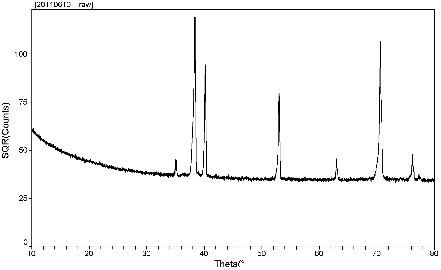
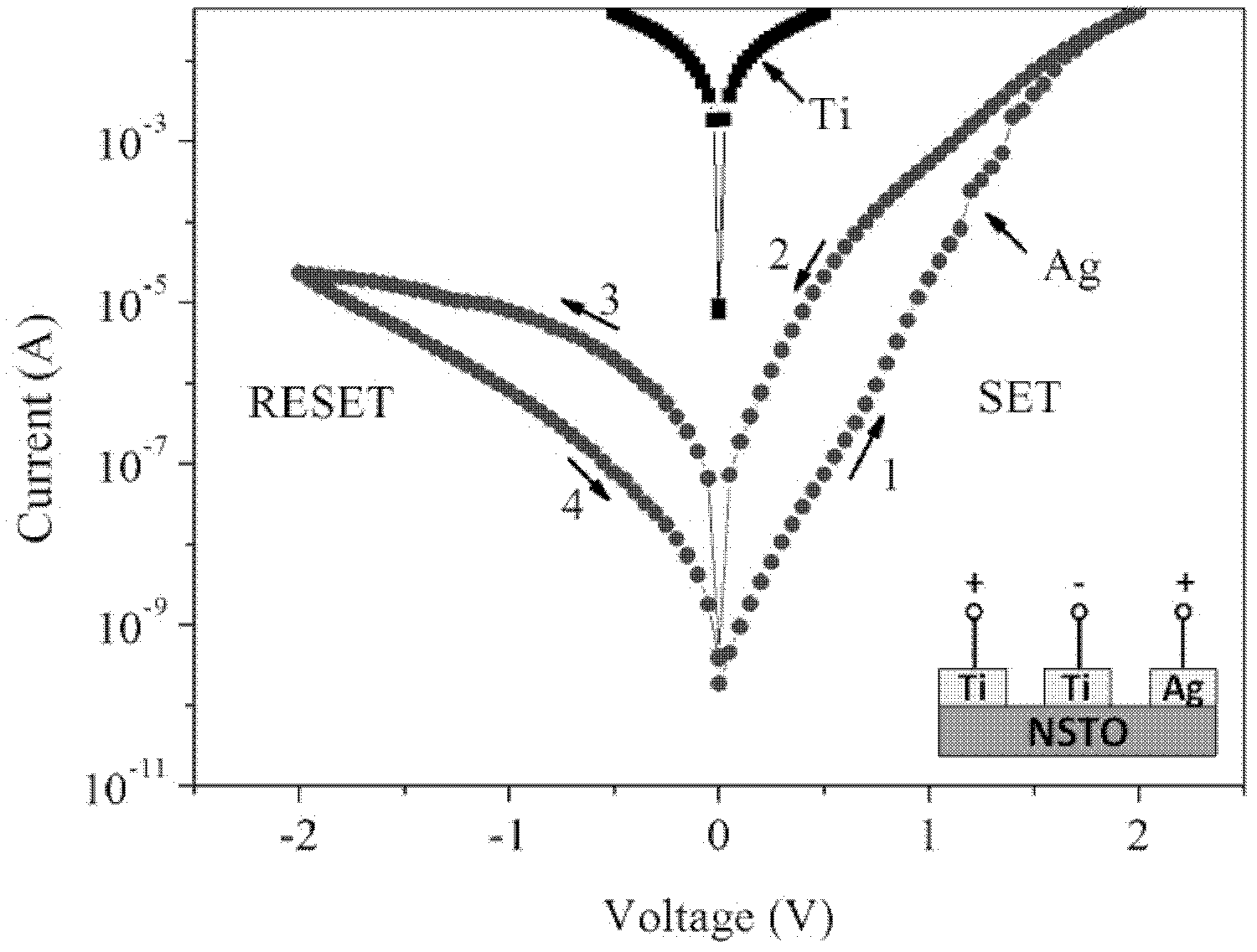
[0023] Take a piece of Nb:SrTiO with a size of 10mm×5mm×0.5mm 3 As the substrate, it was ultrasonically cleaned in deionized water, acetone, deionized water, ethanol, and deionized water, and dried naturally. The substrate was placed in a vacuum of 8 x 10 -4 pa, annealed at 700°C for 30 minutes and then cooled down to room temperature naturally. Then the middle part of the substrate is blocked with a mask, and the exposed Nb:SrTiO 3 A metal titanium (Ti) film with a thickness of 180nm was sputtered, and its X-ray diffraction (XRD) and scanning electron microscope (SEM) showed figure 1 , figure 2 . Then remove the mask plate, in Nb:SrTiO 3 Coated with metallic silver (Ag glue). Metal titanium (Ti) and titanium (Ti) are connected in series with metal copper wire (Cu) and metal titanium (Ti) and metal silver (Ag) are connected in series with metal copper wire (Cu), and metal silver (Ag) is used as For the positive electrode, test their I-V characteristics respectively for...

Embodiment 2

[0025] Take a piece of Nb:SrTiO with a size of 10mm×5mm×0.5mm 3 is the substrate, where Nb:SrTiO 3 SrTiO doped with 0.7% Nb 3 Single crystal substrates were ultrasonically cleaned in deionized water, acetone, deionized water, ethanol, and deionized water. The ultrasonic cleaning time was 5 min, 10 min, 5 min, 10 min, and 5 min, respectively; and then dried naturally. The substrate was placed in a vacuum of 8 x 10 -4 pa, annealed at 700°C for 30 minutes and then cooled down to room temperature naturally. Then cover one-third of the middle part of the substrate with a mask, and use the method of radio frequency magnetron sputtering on the exposed Nb:SrTiO 3 Sputter a layer of metal titanium (Ti) film with a thickness of 160nm, the sputtering power used is 250W, the sputtering pressure is 1.2pa, and the sputtering time is 1.5h; then the mask plate is removed, and the Nb:SrTiO 3 Coated with metallic silver (Ag glue). Metal titanium (Ti) and titanium (Ti) are connected in seri...


PUM

PropertyMeasurementUnit
Thicknessaaaaaaaaaa

Abstract

The invention discloses a resistive random access memory device based on interface oxygen vacancy to achieve the performance of multilevel memory. Specifically, the memory structure utilizes argentums (Ag) and titanium (Ti) as an upper electrode and a lower electrode respectively, utilizes Nb: SrTiO3 as a resistive layer to achieve the performance of multilevel memory. By aid of a magnetron sputtering method, the method for producing resistive random access memory device capable of multilevel memory includes sputtering titanium thin films on Nb: SrTiO3 substrates, coating argentums ( Ag adhesive), obtaining the memory device with an Ag / Nb: SrTiO3 / Ti structure and achieving the performance of multilevel memory. The method for producing resistive random access memory device capable of multilevel memory has the advantages of achieving the excellent performance of multilevel memory by regulating the height of potential barriers through the oxygen vacancy at different positive and negative bias voltages.

Description

technical field [0001] The invention relates to a preparation method of a resistive variable memory device based on interfacial oxygen vacancies to realize multi-valued storage performance, specifically referring to metal Ag and Ti as upper and lower electrodes, and Nb:SrTiO 3 It is the realization of the multi-value storage performance of the storage structure of the resistive variable layer. technical background [0002] High density and low cost are an important goal of memory development. There are three ways to increase memory density: 1) reducing the area of ​​memory cells; 2) 3D integration technology; 3) multi-valued storage technology. Among them, for the technology of increasing the storage unit density per unit chip area by reducing the size, since the process size of the mainstream Flash memory on the market can already be below 65nm, it is difficult to continue to increase the storage density of the memory chip on a large scale. . As for 3D integration techno...

Claims


Application Information

Patent Timeline
IPC IPC(8): H01L45/00
Inventor 李培刚申婧翔张岩王顺利唐为华
Owner ZHEJIANG SCI-TECH UNIV
Learn More