

Method for preparing tin selenide photoelectric thin film
A photoelectric thin film and tin selenide technology, which is applied in the manufacture of circuits, electrical components, and final products, can solve the problems of high preparation costs and complicated process routes, and achieve the effects of low production costs, low requirements for equipment, and easy operation
- Summary
- Abstract
- Description
- Claims
- Application Information
AI Technical Summary
Problems solved by technology
Method used
Image

Examples
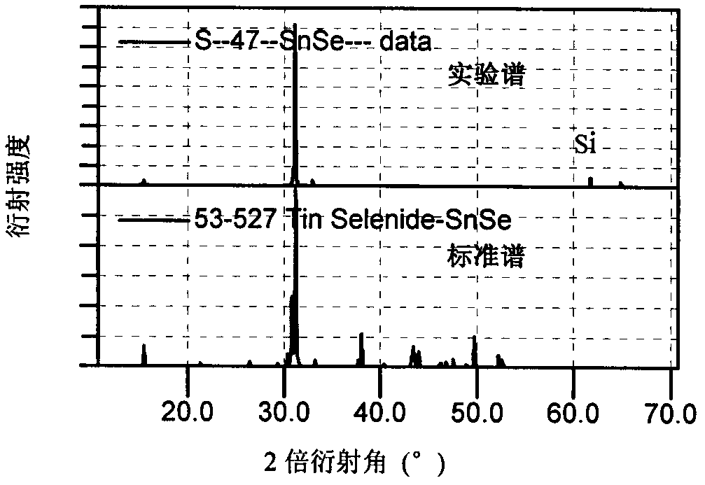
Embodiment 1
[0029] a. Cleaning of the substrate: The silicon substrate (size 2mm×2mm) was cleaned as described above.
[0030] b. 2.036 parts of SnCl 2 2H 2 O and 1.0 parts SeO 2 Put it into a glass bottle, add 54.545 parts of ethanol, and use ultrasonic vibration for more than 30 minutes to make the substances in the solution evenly mixed.
[0031] c. Drop the above solution onto the silicon substrate placed on the homogenizer, and then start the homogenizer. The homogenizer rotates at 200 rpm for 5 seconds, and at 1000 rpm for 15 seconds, so that the dripped solution is coated After the cloth is uniform, the substrate is dried at 100°C, and then the aforementioned solution is repeatedly dripped and spin-coated, and then dried again. This is repeated 8 times, and a precursor thin film sample with a certain thickness is obtained on the substrate.
[0032] d. Put the precursor thin film sample obtained by the above process into an airtight container, and put 18.182 parts of hydrazine hy...
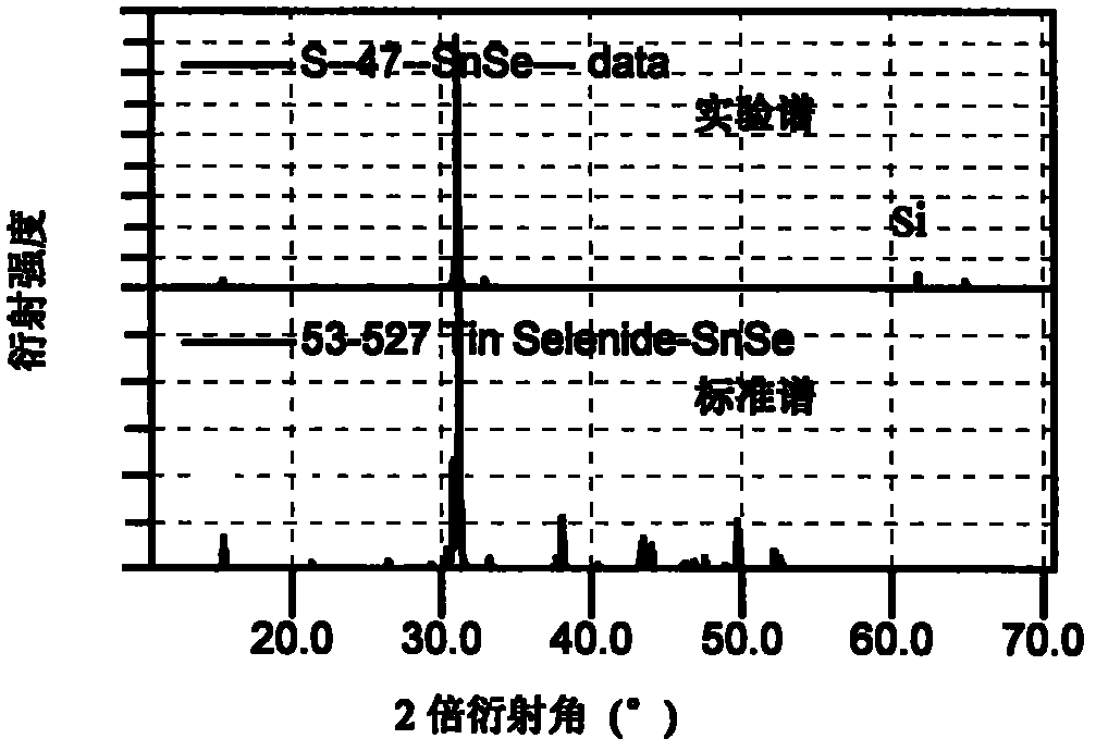
Embodiment 2
[0035] a. Cleaning of the substrate: The silicon substrate (size 2mm×2mm) was cleaned as described above.
[0036] b. 2.036 parts of SnCl 2 2H 2 O and 1.0 parts SeO 2 Put it into a glass bottle, add 54.545 parts of ethanol, and use ultrasonic vibration for more than 30 minutes to make the substances in the solution evenly mixed.
[0037]c. Drop the above solution onto the silicon substrate placed on the homogenizer, then start the homogenizer, rotate the homogenizer at 200 rpm for 5 seconds, and rotate at 3000 rpm for 15 seconds, so that the dripped solution is coated After the cloth is uniform, the substrate is dried at 100°C, and then the aforementioned solution is dripped and spin-coated again, and then dried again. This is repeated 8 times, and a precursor thin film sample with a certain thickness is obtained on the silicon substrate.
[0038] d. Put the precursor thin film sample obtained by the above process into an airtight container, and put 18.182 parts of hydrazin...
PUM
 Abstract
Description
Claims
Application Information