Short-range surface plasma waveguide and dielectric waveguide mixed coupling array type structure

A surface plasmon and surface plasmon wave technology, applied in the field of optoelectronics, can solve the problem of small sensing range

Active Publication Date: 2012-07-25
TSINGHUA UNIV
View PDF2 Cites 8 Cited by
  • Summary
  • Abstract
  • Description
  • Claims
  • Application Information

AI Technical Summary

Problems solved by technology

[0006] The purpose of the present invention is to provide a short-range surface plasmon waveguide and dielectric waveguide hybrid coupling array structure to realize the real-time detection of the adjustable sensing range of the refractive index of the ultra-thin layer medium, while ensuring high sensitivity and stability. The problem of the small sensing range of the traditional waveguide-type surface plasmon wave refractive index detection method is solved

Method used


Image

  • Short-range surface plasma waveguide and dielectric waveguide mixed coupling array type structure
  • Short-range surface plasma waveguide and dielectric waveguide mixed coupling array type structure
  • Short-range surface plasma waveguide and dielectric waveguide mixed coupling array type structure

Examples


Embodiment 1

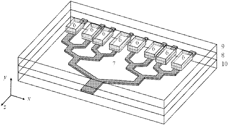
[0041] Figure 5 Shown is a structural diagram of an embodiment of a short-range surface plasmon waveguide and dielectric waveguide hybrid coupling array sensing structure. In this embodiment, the material of the dielectric substrate layer 10 is selected as SiO 2 , the material of the dielectric waveguide layer 7 is Si 3 N 4 , the material of the short-range surface plasmon waveguide layer 6 is Au, and the material of the dielectric covering layer 9 is SiO 2 , the material of the coupling matching layer 8 is SiO2 . On the dielectric substrate layer 10, Si with a width of 2.5 μm-5 μm and a thickness of 180 nm is produced by sputtering or evaporation and photolithography. 3 N 4 Bar 7, a layer of 1.5 μm thick SiO 2 After coupling the matching layer 8, a layer of Au film 6 with a thickness of 15nm-30nm and a length of 30μm-150μm is sputtered on it, and finally a layer of 2μm SiO 2 As a dielectric cover layer 9. Directly above the short-range surface plasmon waveguide layer...

Embodiment 2

[0055] Figure 7 Shown is a three-dimensional structure diagram of another embodiment of a short-range surface plasmon waveguide and a dielectric waveguide hybrid coupling array sensing structure. In this embodiment, the material of the dielectric substrate layer 10 is selected as SiO 2 , the material of the dielectric waveguide layer 7 is Si 3 N 4 , the material of the short-range surface plasmon waveguide layer 6 is Al, and the material of the dielectric covering layer 9 is SiO 2 , the material of the coupling matching layer 8 is SiO 2 . On the dielectric substrate layer 10, Si with a width of 2.5 μm-5 μm and a thickness of 146 nm is produced by sputtering or evaporation and photolithography. 3 N 4 Bar 7, a layer of 2 μm thick SiO 2 After coupling the matching layer 8, sputter a layer of 15nm-30nm thick Al film 6 on it, and finally cover a layer of 3μm SiO 2 As a media overlay. When the incident wavelength is 1550 nm, the width of the dielectric waveguide layer 7 is...

Embodiment 3

[0057] Another example of hybrid coupling array sensing structure of short-range surface plasmon waveguide and dielectric waveguide is as follows. When the incident wavelength is 850nm, Figure 9 Shown is a structure diagram of another embodiment of the short-range surface plasmon waveguide and dielectric waveguide hybrid coupling array sensing structure. The material of the dielectric substrate layer 10 is selected as SiO 2 , the material of the dielectric waveguide layer 7 is PET (polyethylene terephthalate), the material of the short-range surface plasmon waveguide layer 6 is Au, and the material of the dielectric cover layer 9 is SiO 2, the material of the coupling matching layer 8 is SiO 2 . On the dielectric substrate layer 10, a strip 7 of organic material PET with a width of 10 μm-15 μm and a thickness of 1 μm is produced by sputtering or evaporation and photolithography, and a layer of SiO with a thickness of 1.7 μm 2 After coupling the matching layer 8, sputter a...


PUM


Abstract

The invention relates to a short-range surface plasma waveguide and dielectric waveguide mixed coupling array type structure which is characterized in that the coupling array type structure comprises a dielectric substrate layer and at least two coupling structures located on the dielectric substrate layer, wherein each of the coupling structures comprises a dielectric waveguide layer and a short-range surface plasma waveguide layer; the dielectric waveguide layer is located on the dielectric substrate layer; the short-range surface plasma waveguide layer is located on the dielectric waveguide layer; and the short-range surface plasma waveguide layer of at least one of the coupling structure and the short-range surface plasma waveguide layer of the other coupling structure are different in thickness. The structure can be used for realizing a high-sensitivity detection chip with an ultrathin material refractive index in a big sensing area.

Description

technical field [0001] The invention relates to the field of optoelectronic technology, in particular to a hybrid coupling array structure of a short-range surface plasmon waveguide and a dielectric waveguide. Background technique [0002] Surface plasmon polarization (SPP) is an electromagnetic field that propagates along the interface between metal and medium. Such as figure 1 As shown, 1 is the metal (or the mixture of metal and medium), 2 is the medium around the metal, and 3 is the surface plasma wave at an interface. [0003] When the metal film is thinner, the upper and lower surface plasmon waves will be coupled to generate two new surface plasmon wave modes, see figure 2 shown. One of the modes is the anti-symmetric mode, such as figure 2 As shown in middle 5, its mode field is more attached to the metal than the general SPP wave, and the propagation loss is larger, and it can only propagate a short distance along the metal film, which is called short range su...

Claims


Application Information

Patent Timeline
Patent Type & Authority Applications(China)
IPC IPC(8): G02B6/122
Inventor 刘仿樊博宇黄翊东张巍冯雪崔开宇
Owner TSINGHUA UNIV
Why Eureka
Try Eureka