Preparation method for Ge-on-insulator substrate

A germanium substrate and insulator technology, applied in the field of new semiconductor materials, can solve the problems affecting the performance of MOS devices, immature process technology, high interface state density, etc., to suppress the short channel effect, improve the quality of the back interface, and reduce the dielectric constant effect

Inactive Publication Date: 2012-07-25
PEKING UNIV
View PDF4 Cites 11 Cited by
  • Summary
  • Abstract
  • Description
  • Claims
  • Application Information

AI Technical Summary

Problems solved by technology

However, these two technologies for preparing germanium-on-insulator (GeOI) substrates are immature, and the prepared germanium-on-insulator (GeOI) substrates have a common shortcoming, that is, the upper germanium film and the buried oxide (BOX) layer. The quality of the interface (back interface) is too poor, there are a large number of dangling bonds, and the interface state density is very high, which seriously affects the performance of MOS devices based on germanium-on-insulator (GeOI) substrates

Method used


Image

  • Preparation method for Ge-on-insulator substrate
  • Preparation method for Ge-on-insulator substrate
  • Preparation method for Ge-on-insulator substrate

Examples


Embodiment Construction

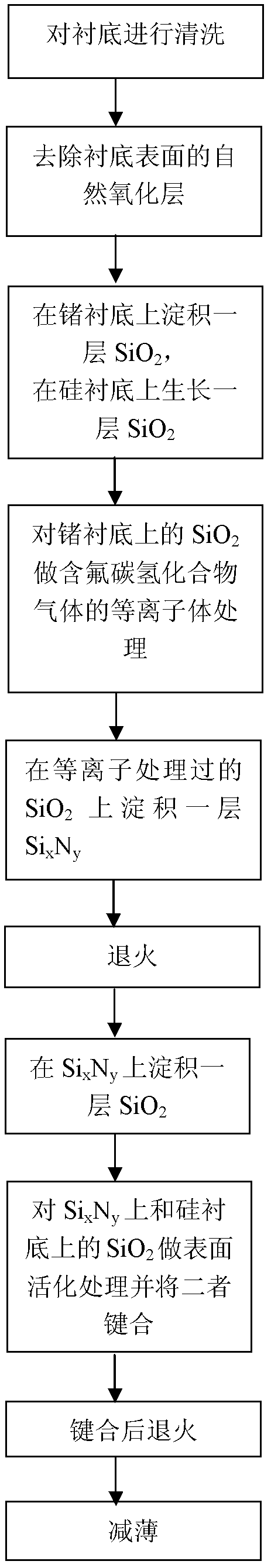
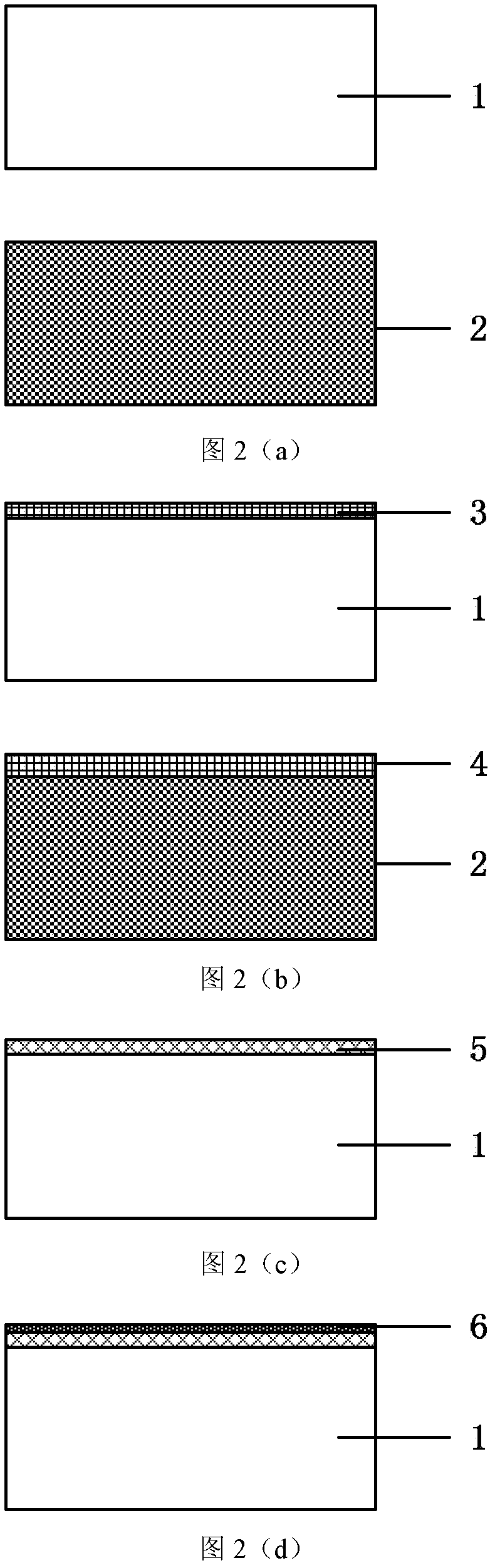
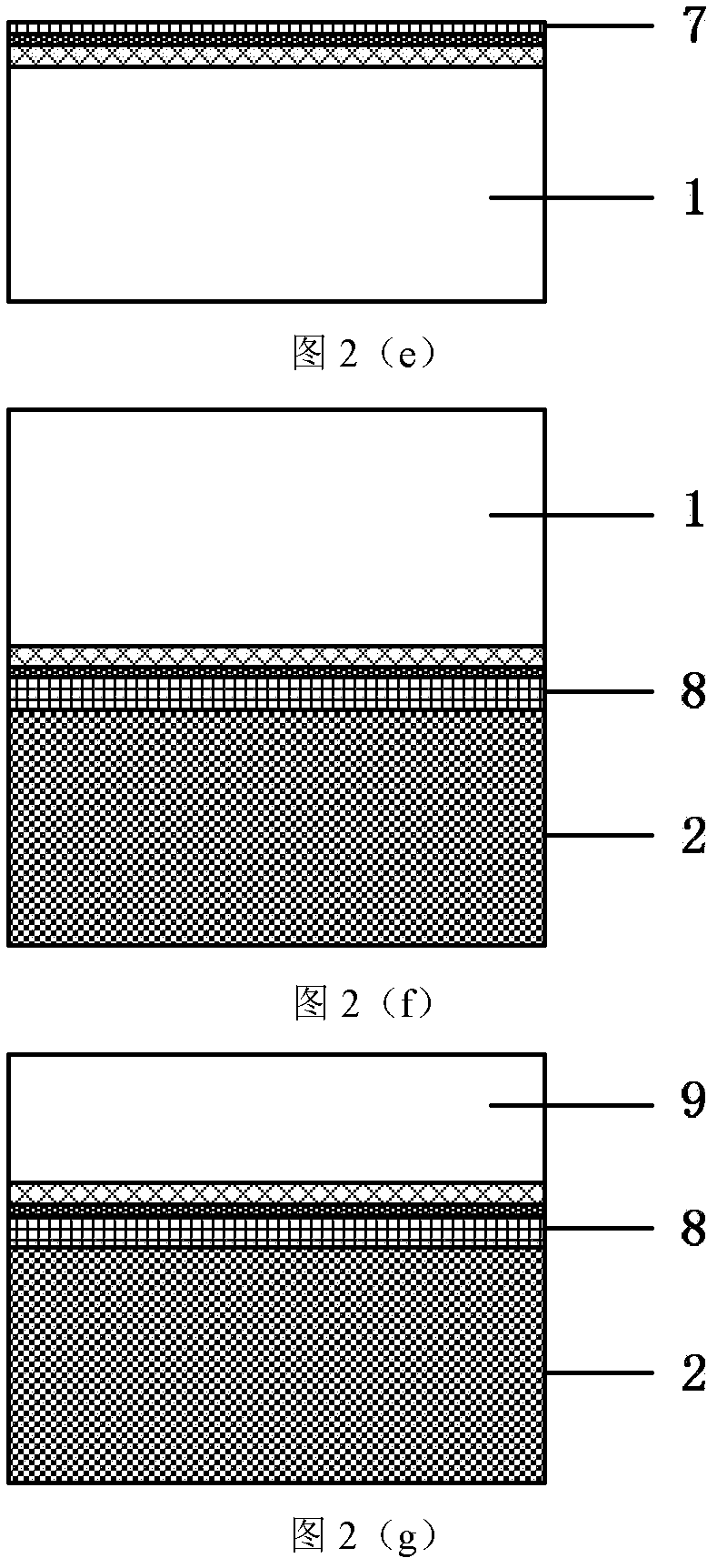
[0031] The following examples illustrate the present invention, but these examples should not be construed as limiting the present invention.

[0032] Step 1. Select semiconductor germanium substrate and silicon substrate, such as figure 2 Shown in (a); the germanium substrate and the silicon substrate are cleaned. Firstly, organic cleaning is performed on the germanium substrate, followed by soaking and cleaning with acetone and ethanol, and then flushing with DI water to remove oil stains and organic pollutants on the germanium substrate. Then wash with hydrochloric acid, heat and boil in dilute hydrochloric acid, then rinse with DI water to remove inorganic pollutants, metal particles, etc.; first use No. 1 cleaning solution (NH 4 OH: H 2 O 2 : H 2 O=1:1:5~1:2:7) The silicon substrate is cleaned, and then cleaned with deionized water to remove particles and organic substances on the substrate. Use No. 2 cleaning solution (HCl:H 2 O 2 : H 2 O=1:1:6~1:2:8) cleaning, and then c...


PUM

PropertyMeasurementUnit
thicknessaaaaaaaaaa

Abstract

The invention discloses a preparation method for a Ge-on-insulator (GeOI) substrate and belongs to the field of semiconductor devices. Passvating treatment is realized on an interface of a Ge film of the upper layer and a buried oxygen layer in the process of preparing the GeOI substrate in the method, and thereby, the state density of the interface is reduced, and the quality of the back interface of the GeOI substrate is increased. The preparation method for the GeOI substrate is capable of effectively reducing the dielectric constant of the buried oxygen (BOX) layer and is favorable of restraining a short-channel effect of a metal-oxide-semiconductor field effect transistor (MOSFET) prepared based on the GeOI substrate.

Description

Technical field [0001] The invention belongs to the field of new semiconductor materials, and specifically relates to a method for preparing a germanium substrate on an insulator. Background technique [0002] As the feature size of traditional bulk silicon MOS devices shrinks to the nanometer scale, the method of improving the operating speed by reducing the geometric size of the device is facing the double test of the physical and technological limits of transistor size. In order to continue to improve the working speed of the device, it is necessary to find new materials and adopt new device structures. Due to its high carrier mobility, germanium is considered to be one of the candidate materials to realize the next generation of high-speed MOSFET. At room temperature (300K), the electron mobility of germanium material is 2.4 times that of silicon, and the hole mobility is 4 times that of silicon. Similarly, with the shrinking of the device geometry, the performance degradat...

Claims


Application Information

Patent Timeline
Patent Type & Authority Applications(China)
IPC IPC(8): H01L21/762
Inventor 黄如林猛安霞张兴
Owner PEKING UNIV
Why Eureka
Try Eureka