Pixel array substrate

A pixel array substrate, substrate technology, applied in the direction of optics, instruments, electrical components, etc., can solve the problems of inability to reduce the display pixel area, increase the capacitance plane area, and improve the screen resolution, etc., to achieve the reduction of backlight brightness and pixel size The effect of miniaturization and area reduction

Active Publication Date: 2012-08-01
AU OPTRONICS CORP
View PDF7 Cites 22 Cited by
  • Summary
  • Abstract
  • Description
  • Claims
  • Application Information

AI Technical Summary

Problems solved by technology

[0004] Therefore, for Organic Light Emitting Diode (OLED) displays, when more thin-film transistors are required for each pixel, it is difficult to increase the capacitor plane area in order to obtain high resolution. If the plane area of ​​the capacitor cannot be reduced, it will be difficult to increase the screen resolution in order to obtain the charge storage capacity that can maintain the normal display screen
On the other hand, displays such as electronic paper (Electronic paper) require a large capacitance design to maintain the gray scale of the display screen. resolution limited

Method used


Image

  • Pixel array substrate
  • Pixel array substrate
  • Pixel array substrate

Examples


Embodiment Construction

[0063] Figure 2A to Figure 2G It is a schematic cross-sectional view of the manufacturing process of the pixel array substrate according to an embodiment of the present invention.

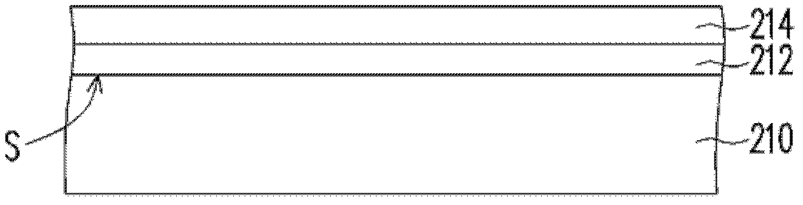
[0064] Please refer to Figure 2A A first sub-insulation layer 212 and a second sub-insulation layer 214 are sequentially formed on a surface S of a substrate 210 . In this embodiment, the substrate 210 is, for example, a glass substrate, and the material of the first sub-insulation layer 212 is, for example, silicon nitride (SiN x ), and the material of the second sub-insulation layer 214 is, for example, silicon oxide (SiO x ), but the present invention is not limited thereto.

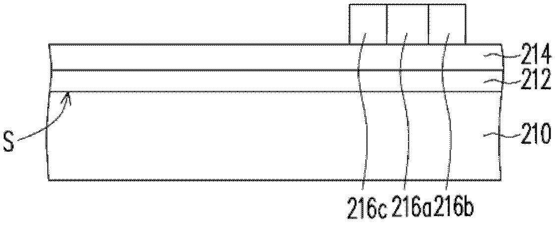
[0065] Please refer to Figure 2B , forming a channel material layer (not shown) on the second sub-insulation layer 214 . The material of the channel material layer can be low temperature polysilicon or amorphous silicon. In this embodiment, the material of the channel layer is low-temperature polysilicon, wherein th...


PUM


Abstract

The invention discloses a pixel array substrate, comprising a substrate, multiple scanning lines, multiple data lines, multiple collective lines, multiple capacitors, multiple active elements and multiple pixel electrodes. The substrate has a surface. The multiple scanning lines, the multiple data lines and the multiple collective lines are arranged on the substrate. The multiple capacitors are configured on the substrate and are coupled to the collective lines. A relative surface of a top electrode of each capacitor is uneven. The multiple active elements are arranged on the substrate. The multiple pixel electrodes are disposed on the substrate, and each pixel electrode is electrically connected with the corresponding scanning line and the corresponding data line via different active elements.

Description

technical field [0001] The present invention relates to a substrate, and in particular to a pixel array substrate. Background technique [0002] Multimedia technology in today's society is quite developed, mostly benefiting from the progress of semiconductor components and displays. As far as displays are concerned, thin film transistor liquid crystal displays with superior characteristics such as high image quality, low power consumption, and no radiation have gradually become the mainstream of the market. [0003] With people's demand for high resolution of the display, the area of ​​each pixel (pixel) in the display must be reduced, and the area of ​​the components of the display must also be reduced. However, if figure 1 As shown, most of the capacitor designs currently on the market are planar structures. Specifically, by forming a first electrode 112 and a second electrode 116 on the substrate 110, and disposing an insulating layer 114 between the first electrode 11...

Claims


Application Information

Patent Timeline
IPC IPC(8): H01L27/02G02F1/1362G02F1/1368
Inventor 彭尧
Owner AU OPTRONICS CORP
Why Eureka
Try Eureka