Transistor constructions and electronic devices

a transistor and electronic device technology, applied in the field of integrated circuits, can solve the problems of limited performance of tfts, limited carrier mobilities, high power consumption, etc., and achieve the effects of convenient use, convenient and fast charging, and low power consumption

Inactive Publication Date: 2005-11-10
MICRON TECH INC
View PDF27 Cites 10 Cited by
  • Summary
  • Abstract
  • Description
  • Claims
  • Application Information

AI Technical Summary

Benefits of technology

[0012] In further aspects of the prior art, known dynamic random access memory (DRAM) devices include a switching transistor and an integrated storage capacitor tied to the storage node of the transistor. Incorporating a stacked capacitor or a trench capacitor in parallel with the depletion capacitance of the floating storage node enhances charge storage. Due to a finite charge leakage across the depletion layer, the capacitor is frequently recharged or refreshed to ensure data integrity in the DRAM device. Thus, such a DRAM device is volatile. A power failure causes permanent data loss in a DRAM device. DRAM devices are relatively inexpensive, power efficient, and fast compared to non-volatile random access memory (NVRAM) devices.

Problems solved by technology

A problem associated with conventional TFT constructions is that grain boundaries and defects can limit carrier mobilities.
High voltage (and therefore high power consumption), and large areas are utilized for the TFTs, and the TFTs exhibit limited performance.
TFTs thus have limited commercial application and currently are utilized primarily for large area electronics.
Performance enhancements of standard field effect transistor devices are becoming limited with progressive lithographic scaling in conventional applications.
Although various techniques have been developed for substantially controlling nucleation and grain growth processes of semiconductor materials, grain orientation control is lacking.
Further, the post-anneal treatment utilized in conjunction with MILC can be unsuitable in applications in which a low thermal budget is desired.
Thus, such a DRAM device is volatile.
A power failure causes permanent data loss in a DRAM device.
A significant challenge for every succeeding generation of reduced feature size is to provide this minimum capacitance per cell.
However, these complex three-dimensional capacitor structures are difficult to manufacture and adversely impact yield.
There has been serious concern of the scalability of the conventional DRAM cell beyond the 0.1 μm lithographic generation.
The scaling problems have been aggravated by increased device short channel effects and leakages associated with complicated capacitor structures.
Therefore, controlling the memory retention between refresh operations is expected to be difficult.
Field emission across the surrounding insulator causes the stored charge to leak.
However, there are problems associated with NVRAM devices.
The writing process, also referred to as “write-erase programming,” for non-volatile memory is slow and energy inefficient, and requires complex high voltage circuitry for generating and routing high voltage.
The degradation of the insulator eventually causes significant leakage of the stored charge.
Thus, the high-field phenomena negatively affects the endurance (the number of write / erase cycles) of the NVRAM devices.
Therefore, the available applications for these known NVRAM devices is limited.

Method used


Image

  • Transistor constructions and electronic devices
  • Transistor constructions and electronic devices
  • Transistor constructions and electronic devices

Examples


Embodiment Construction

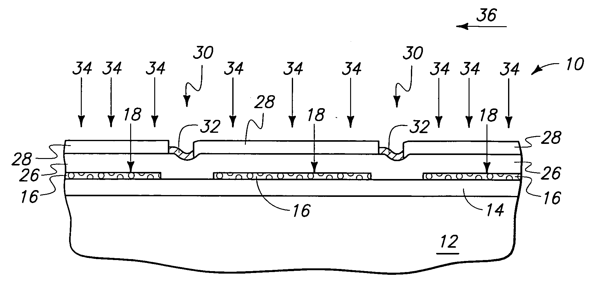
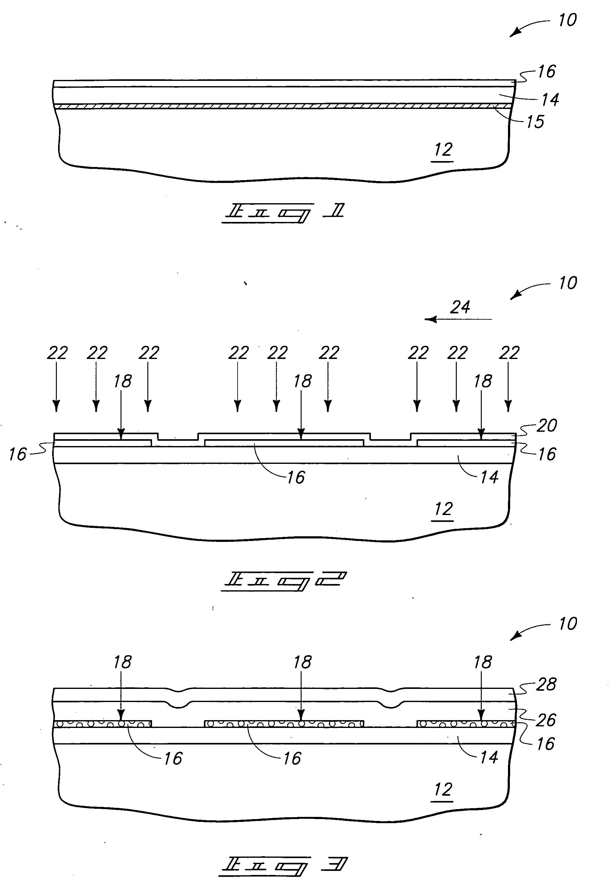
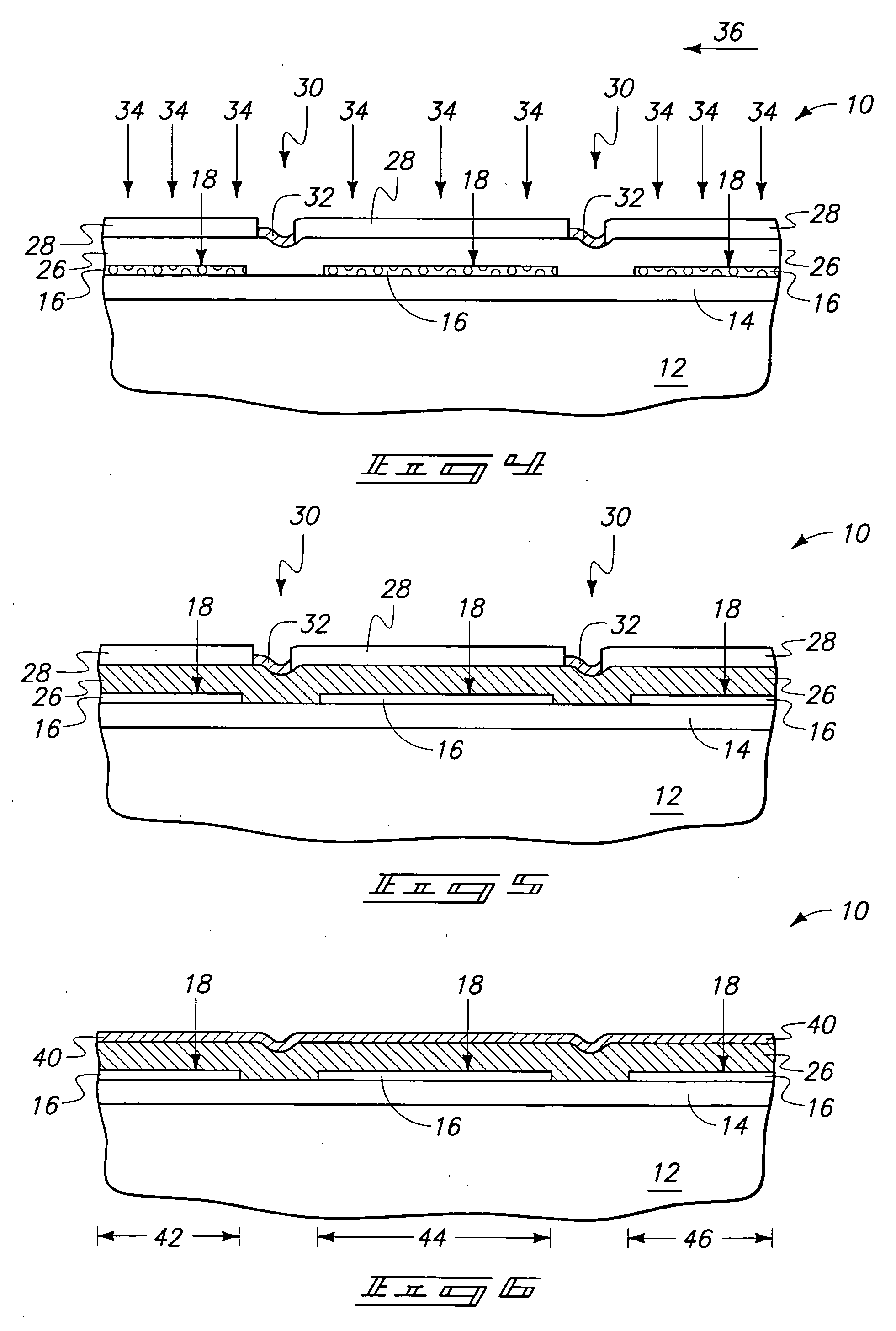
[0054] The invention pertains to memory devices less volatile than conventional DRAM, and in particular aspects pertains to non-volatile memory devices. In various aspects, the invention pertains to incorporation of active regions of partially-depleted SOI field effect transistor (PD-SOI-FET) devices within Si / Ge materials, and in further aspects the invention encompasses incorporation of non-volatile memory devices in SOI constructions utilizing Si / Ge as a semiconductor material. Exemplary PD-SOI-FET devices are described with reference to FIGS. 10-28. Prior to the discussion of the exemplary PD-SOI-FET devices, a processing sequence for forming and utilizing preferred Si / Ge materials is described with reference to FIGS. 1-9, with particular aspects of the invention comprising forming a PD-SOI body over any versatile substrate base, including, for example, glass, metal, plastic semiconductive materials, alumina, silicon dioxide, etc.

[0055] Referring to FIG. 1, a fragment of a semi...


PUM


Abstract

The invention includes a non-volatile memory cell comprising a field effect transistor construction having a body region within a crystalline material. The body region includes a charge trapping region. The memory cell can be TFT-SOI based, and can be supported by a substrate selected from a diverse assortment of materials. The top portion of the substrate can be a conductive layer separated from the memory device by the SOI-oxide insulator film. The charge trapping region can be, for example, silicon enriched silicon nitride or silicon enriched silicon oxide. The crystalline material can include silicon and germanium. The transistor comprises first and second diffusion regions within the body region, and also comprises a channel region between the first and second diffusion regions. The entirety of the body region within the crystalline material can be within a single crystal of the material.

Description

TECHNICAL FIELD [0001] This disclosure relates generally to integrated circuits. In particular aspects, the invention pertains to non-volatile, semiconductor-on-insulator (SOI) memory cells. In particular aspects, the memory cells are SOI-thin film transistor based, built over a versatile base (or substrate). BACKGROUND OF THE INVENTION [0002] SOI technology differs from traditional bulk semiconductor technologies in that the active semiconductor material of SOI technologies is typically much thinner than that utilized in bulk technologies. The active semiconductor material of SOI technologies will typically be formed as a thin film over an insulating material (typically oxide), with exemplary thicknesses of the semiconductor film being less than or equal to 2000 Å. In contrast, bulk semiconductor material will typically have a thickness of at least about 200 microns. The thin semiconductor of SOI technology can allow higher performance and lower power consumption to be achieved in ...

Claims


Application Information

Patent Timeline
Patent Type & Authority Applications(United States)
IPC IPC(8): G11C16/04G11C16/10G11C16/26G11C16/28H01L21/02H01L21/336H01L21/768H01L21/8242H01L21/8246H01L21/8247H01L21/84H01L27/108H01L27/115H01L27/12H01L29/786H01L29/788
CPCG11C16/0416H01L29/7881G11C16/26G11C16/28G11C2211/4016H01L21/76838H01L21/84H01L27/10802H01L27/10814H01L27/10852H01L27/10873H01L27/115H01L27/11521H01L27/11568H01L27/12H01L27/1203H01L28/40H01L29/66742H01L29/66825H01L29/66833H01L29/7841H01L29/7842H01L29/78687G11C16/10H10B12/20H10B12/315H10B12/05H10B12/033H10B43/30H10B69/00H10B41/30
Inventor BHATTACHARYYA, ARUP
Owner MICRON TECH INC
Why Eureka
Try Eureka